Semiconductor structure and forming method thereof

A technology of semiconductor and gate structure, which is applied in the field of semiconductor structure and its formation, can solve the problems that the electrical performance of semiconductor devices needs to be improved, and achieve the effects of reducing body region leakage current, improving electrical performance, and increasing diffusion distance

Inactive Publication Date: 2018-05-25
SEMICON MFG INT (SHANGHAI) CORP +1
View PDF7 Cites 6 Cited by
  • Summary
  • Abstract
  • Description
  • Claims
  • Application Information

AI Technical Summary

Problems solved by technology

[0006] However, the electrical performance of the formed semiconductor device still needs to be improved after adopting the metal silicide layer technology.

Method used


Image

  • Semiconductor structure and forming method thereof
  • Semiconductor structure and forming method thereof
  • Semiconductor structure and forming method thereof

Examples


Embodiment Construction

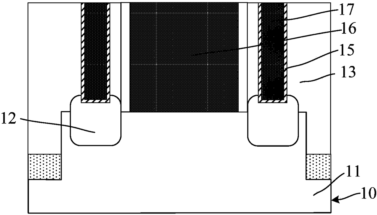
[0016] It can be known from the background art that after adopting the metal silicide layer technology, the electrical performance of the formed semiconductor device still needs to be improved. refer to figure 1 , shows a schematic structural diagram corresponding to a method for forming a semiconductor structure. The reason why the electrical performance of the formed semiconductor device still needs to be improved is analyzed in combination with a method for forming a semiconductor structure.

[0017] The forming method includes: forming a base 10, the base 10 includes a substrate 11, a gate structure 16 on the substrate 11, and source-drain doped epitaxy in the base 10 on both sides of the gate structure 16. layer 12, and a dielectric layer 13 located on the substrate 10 exposed by the gate structure 16; contact openings (not shown) exposing the source-drain doped epitaxial layer 12 are formed on both sides of the gate structure 16, The contact opening includes a through ...


PUM


Abstract

The invention discloses a semiconductor structure and a forming method thereof. The method comprises the steps of forming a substrate, wherein the substrate comprises a substrate, a gate structure located on the substrate, source-drain doped regions located in the substrate at two sides of the gate structure, and a dielectric layer located on the substrate from which the gate structure is exposed;forming contact openings for exposing the source-drain doped regions in two sides of the gate structure, wherein each contact opening comprises a through hole penetrating through the substrate with the thickness of the dielectric layer, and a groove penetrating through the substrate with the thickness of the part corresponding to each source-drain doped region, and the bottom size of each grooveis smaller than the top size in the direction vertical to the extension direction of the gate structure; covering the surfaces of the grooves with a metal silicide layer in a conformal manner; and forming the metal silicide layer and then forming contact hole plugs in the contact openings. The bottom size of each groove is smaller than the top size, so that, compared with a scheme that side wallsof the grooves are vertical to the substrate, the semiconductor structure has the advantages that the diffusion distance from metal atoms to a channel region in the process of forming the metal silicide layer can be increased, and the possibility that the metal atoms are diffused to a bulk region of the substrate is reduced, thereby reducing bulk leakage current.

Description

technical field [0001] The invention relates to the field of semiconductors, in particular to a semiconductor structure and a forming method thereof. Background technique [0002] With the continuous development of integrated circuit manufacturing technology, people's requirements for the integration and performance of integrated circuits are becoming higher and higher. In order to improve integration and reduce costs, the critical dimensions of components are getting smaller and the circuit density inside integrated circuits is increasing. This development makes the surface of the wafer unable to provide enough area to make the required interconnection lines. [0003] In order to meet the requirements of the interconnection line after the critical dimension is reduced, at present, the conduction between different metal layers or between the metal layer and the substrate is realized through the interconnection structure. The interconnection structure includes interconnectio...

Claims


Application Information

Patent Timeline
Patent Type & Authority Applications(China)
IPC IPC(8): H01L21/336H01L21/8238H01L27/092H01L29/78H01L29/06
CPCH01L21/8238H01L27/092H01L29/0607H01L29/0684H01L29/66795H01L29/785H01L21/76805H01L21/76897
Inventor 李勇
Owner SEMICON MFG INT (SHANGHAI) CORP
Why Eureka
Try Eureka