Semiconductor package having high quantity of I/O connections and method for fabricating the same

a technology of i/o connection and semiconductor, which is applied in the direction of semiconductor devices, semiconductor/solid-state device details, electrical apparatus, etc., can solve the problems of degrading the yield of the electrical connection with the external device, and undesirably increasing the fabrication cost, so as to prevent the warpage of the conductive member, increase the length of the lead, and ensure the quality of the wire bonding

Inactive Publication Date: 2005-03-10
SILICONWARE PRECISION IND CO LTD
View PDF7 Cites 46 Cited by
  • Summary
  • Abstract
  • Description
  • Claims
  • Application Information

AI Technical Summary

Benefits of technology

[0016] The at least one conductive member is integrally connected to a side of the die pad. One advantage by this arrangement is that, during a wire-bonding process, the bottom surface of the die pad is sucked by a vacuum socket, allowing the conductive member along with the die pad to be firmly attached to a jig and thereby preventing the conductive member from warpage, such that the quality of wire bonding can be assured. On the contrary, if the conductive member is formed on an inner end of a lead, it increases the length of the lead, and during the wire-bonding process, the inner end of the lead having the conductive member cannot well clamped by the jig and would be subject to warpage, thereby degrading the quality of wire bonding. Therefore, formation of the conductive member on the inner end of the lead is not applicable.

Problems solved by technology

However, reducing the pitch between adjacent leads requires tremendous precision in manufacturing the lead frame and thus undesirably increases the fabrication cost.
Further, when the leads with the reduced pitch are attached to an external device such as printed circuit board (PCB) by surface mounting technique (SMT), short circuit may be easily induced due to the reduced pitch, thereby degrading the yield on the electrical connection with the external device.
However, the increase in size of the encapsulant not only increases the fabrication cost but also easily leads to warpage of the encapsulant, which adversely affects the yield of the fabricated packages.
Further, the encapsulant with the increased size does not comply with current demands for light-weight and low-profile semiconductor packages.
Although the above semiconductor package 1″ may have more I / O connections, fabrication of the lead frame 10″ shown in FIG. 15 is complex and cost-ineffective.
Further, the lead frame 10″ is connected to the peripheral frame 11″ merely using the support bars 103″ provided at the four corners, and the lead frame 10″ is relatively thin, it is usually difficult to maintain the conductive pads 101″ at the outermost and the innermost positions coplanar during a wire-bonding process, thereby resulting in undesirable warpage of the lead frame 10″ and unsatisfactory bonding quality between the outer conductive pads 101″ and the chip 12″ thereon.
As a result, the yield and reliability of the fabricated packages would be reduced.
This problem becomes even more severe in the case of increasing the size of the lead frame for carrying more conductive pads.
Moreover, due to the small size of the conductive pads 101″, it is not applicable to use a jig that is for clamping the outer leads of the conventional lead frame to prevent the occurrence of warpage, and therefore the quality of wire bonding for the lead frame 10″ cannot be assured.
In addition, as mentioned above that the lead frame 10″ is complex and cost-ineffective to fabricate, thus there still remains a need to improve such a semiconductor package 1″.

Method used


Image

  • Semiconductor package having high quantity of I/O connections and method for fabricating the same
  • Semiconductor package having high quantity of I/O connections and method for fabricating the same
  • Semiconductor package having high quantity of I/O connections and method for fabricating the same

Examples


Embodiment Construction

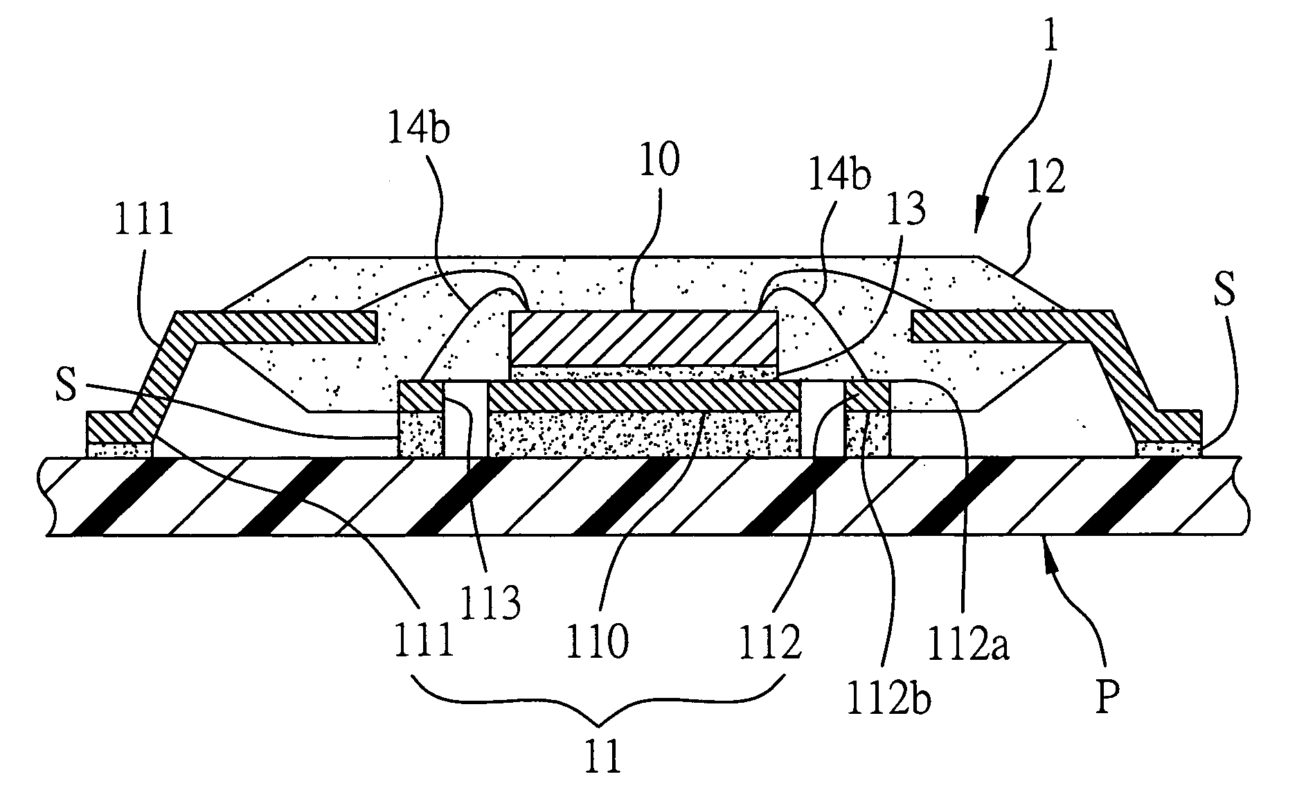
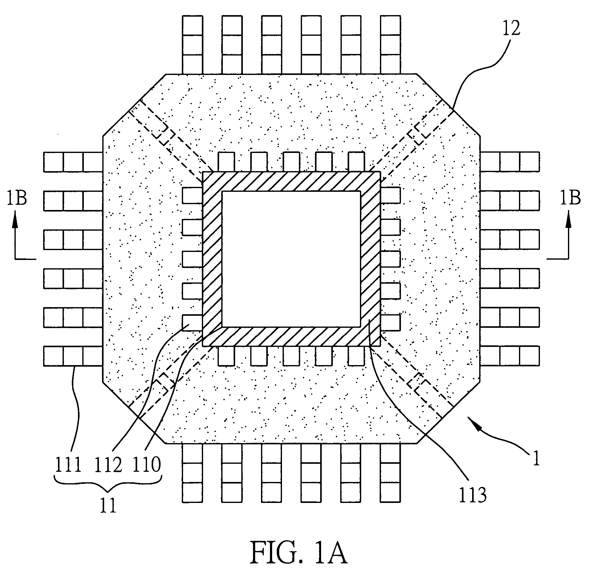
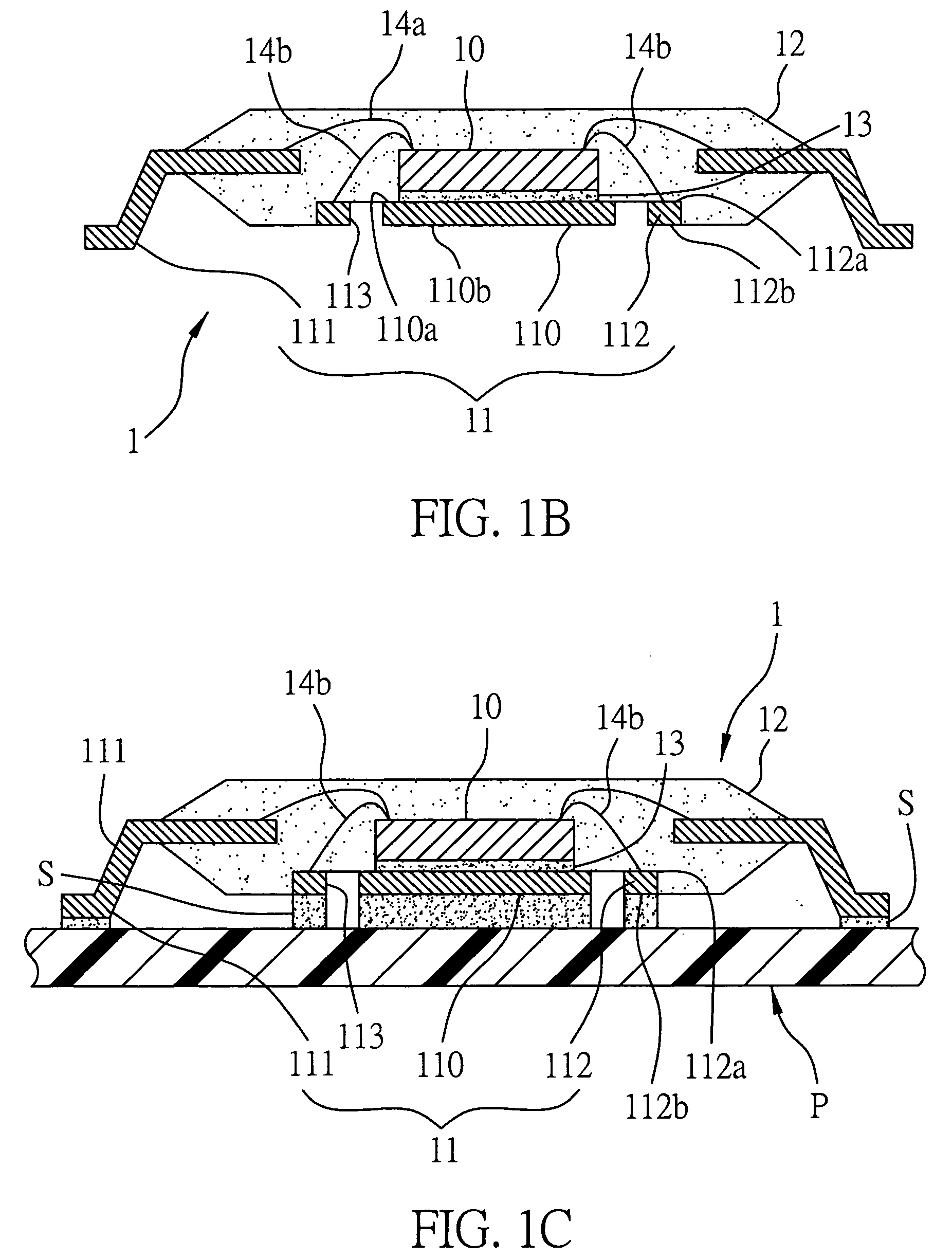
[0035]FIG. 1A shows a bottom view of a semiconductor package having a high quantity of I / O connections in accordance with a first preferred embodiment of the present invention, and FIG. 1B is a cross-sectional view of the semiconductor package in FIG. 1A taken along line 1B-1B.

[0036] As shown in the drawings, the semiconductor package 1 comprises a semiconductor chip 10, a lead frame 11 for carrying the chip 10, and an encapsulant 12 for encapsulating the chip 10 and a portion of the lead frame 11.

[0037] The lead frame 11 comprises a die pad 110, a plurality of leads 111 disposed around the die pad 110, and a plurality of conductive members 112 formed between the die pad 110 and the leads 11, as shown in FIG. 1B. The die pad 110 has a top surface 110a, and a bottom surface 110b opposed to the top surface 110a, wherein the bottom surface 110b is exposed from the encapsulant 12. Similarly, each of the conductive members 112 has a top surface 112a, and a bottom surface 112b opposed t...


PUM


Abstract

A semiconductor package having a high quantity of input/output (I/O) connections and a fabrication method thereof are proposed. A lead frame having a plurality of leads, a die pad and at least one conductive member electrically isolated from the die pad and disposed between the die pad and leads, is provided for at least one semiconductor chip to be mounted on the die pad. The semiconductor chip is electrically connected to the leads and the at least one conductive member. An encapsulant is formed to encapsulate the semiconductor chip and a portion of the lead frame with bottom surfaces of the die pad and the at least one conductive member and a portion of the leads being exposed from the encapsulant. The at least one conductive member electrically separated from the die pad is used as an I/O connection for external connection between the semiconductor chip and external devices.

Description

FIELD OF THE INVENTION [0001] The present invention relates to semiconductor packages, and more particularly to a semiconductor package having a lead frame as a chip carrier and a method for fabricating the same. BACKGROUND OF THE INVENTION [0002] A conventional semiconductor package having a lead frame as a chip carrier is typically provided with a semiconductor chip mounted on a die pad of the lead frame, wherein leads of the lead frame are disposed around the die pad and have outer leads exposed from an encapsulant or mold body that is used for encapsulating the chip and the lead frame, the exposed outer leads serving as input / output (I / O) connections for electrical connection between the semiconductor package and external devices. This type of semiconductor package device is customarily named Quad Flat Package (QFP), which has been developed with various modified configurations as disclosed in U.S. Pat. Nos. 5,397,746, 5,905,299, 5,559,306, 5,923,092 and 5,489,801. [0003] Accord...

Claims


Application Information

Patent Timeline
Patent Type & Authority Applications(United States)
IPC IPC(8): H01L21/48H01L23/495
CPCH01L21/4821H01L2224/32245H01L23/49503H01L2224/48091H01L2224/48247H01L2224/49109H01L2924/01079H01L23/495H01L2224/45144H01L2224/73265H01L24/48H01L24/49H01L2224/48257H01L2224/92247H01L2924/00014H01L2924/00H01L2924/12042H01L24/45H01L2924/181H01L2224/49433H01L2924/00015H01L2224/05599H01L2924/00012
Inventor HSU, CHIN-TENG
Owner SILICONWARE PRECISION IND CO LTD
Why Eureka
Try Eureka