Nanometer-level and high-precision preparation method for cross section of IC product

A high-precision, nano-scale technology, applied in the preparation of test samples, nanostructure manufacturing, nanotechnology and other directions, can solve the problems of low efficiency, low precision, long time consumption, etc., to reduce production costs, high precision, and long service life. short effect

Inactive Publication Date: 2018-07-10
BEIJING SMARTCHIP MICROELECTRONICS TECH COMPANY +2
View PDF9 Cites 3 Cited by
  • Summary
  • Abstract
  • Description
  • Claims
  • Application Information

AI Technical Summary

Problems solved by technology

[0008] The purpose of the present invention is to provide a nanoscale high-precision preparation method for the sample cross-section of an IC product, thereby overcoming the problems of long time-consuming, low efficiency and low precision of the preparation method in the prior art

Method used


Image

  • Nanometer-level and high-precision preparation method for cross section of IC product
  • Nanometer-level and high-precision preparation method for cross section of IC product
  • Nanometer-level and high-precision preparation method for cross section of IC product

Examples


Embodiment Construction

[0024] The specific embodiments of the present invention will be described in detail below in conjunction with the accompanying drawings, but it should be understood that the protection scope of the present invention is not limited by the specific embodiments.

[0025] Unless expressly stated otherwise, throughout the specification and claims, the term "comprise" or variations thereof such as "includes" or "includes" and the like will be understood to include the stated elements or constituents, and not Other elements or other components are not excluded.

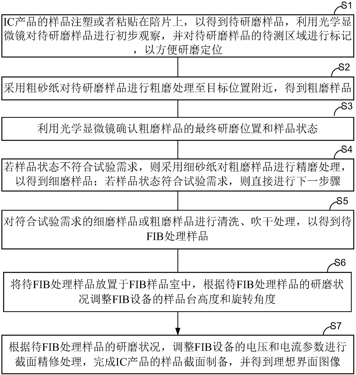
[0026] Such as figure 1 Shown is a flowchart of a nanoscale high-precision preparation method for a sample section of an IC product according to a specific embodiment of the present invention, and the preparation method includes the following steps:

[0027] S1. Injecting or pasting the sample of the IC product on the accompanying sheet to obtain the sample to be ground, using an optical microscope to conduct a preliminary...


PUM

PropertyMeasurementUnit
heightaaaaaaaaaa

Abstract

The invention discloses a nanometer-level and high-precision preparation method for the cross section of an IC product sample. The method comprises the following steps: S1, inject-molding or pasting the IC product sample on a detection sheet to obtain a sample to be ground, preliminarily observing the sample to be ground, and marking an area to be tested; S2, coarsely grinding the sample to be ground by flint paper to obtain a coarsely ground sample; S3, confirming the final grinding position and the sample state of the coarsely ground sample; S4, finely grinding the coarsely ground sample byadopting fine sandpaper if the sample state does not meet test demands; S5, performing cleaning and blow-drying treatment on the finely ground sample or the coarsely ground sample meeting the test demands to obtain a sample to be subjected to FIB treatment; S6, placing the sample to be subjected to FIB treatment in an FIB sample chamber, and adjusting the height and the rotation angle of the sample table of an FIB device; and S7, adjusting the voltage and current parameters of the FIB device, and performing cross-section finishing treatment to complete the sample cross section preparation. Thepreparation method has the advantages of high efficiency and high precision, and allows the identification degree of the section sample to reach a nanometer level.

Description

technical field [0001] The invention belongs to the technical field of chips, and relates to a nanoscale high-precision preparation method for the cross section of an IC product. Background technique [0002] With the rapid development of high integration, refinement, and thinning of integrated circuits, the process size of chips continues to shrink and the packaging density continues to increase. For high-end products with small size and complex process, high-precision sample processing technology is the guarantee for in-depth study of sample structure and materials. Observing the hierarchical structure of the sample and the film thickness of each layer requires the preparation of high-quality sample cross-sections (such as observing the growth of the interface metal compound IMC and its changes before and after the reliability test, and judging the TSV (ThroughSillicon Via, through-silicon via) through-hole The quality of the process and the metallographic structure of th...

Claims


Application Information

Patent Timeline
Patent Type & Authority Applications(China)
IPC IPC(8): G01N1/28B82B3/00B82Y40/00
CPCB82B3/0038B82Y40/00G01N1/286G01N2001/2866
Inventor 乔彦彬李建强陈燕宁邵瑾赵扬刘亮马强窦海啸杨苗苗张萌
Owner BEIJING SMARTCHIP MICROELECTRONICS TECH COMPANY
Why Eureka
Try Eureka