Grid scanning drive circuit

A driving circuit and gate scanning technology, applied in static indicators, instruments, etc., can solve the problems of reducing the maintenance capability of the pull-up control node maintenance module 5, reducing the reliability of the circuit, increasing the complexity of the circuit, and saving layout space. , The effect of improving reliability and reducing the number of TFT components

Active Publication Date: 2018-07-10
NANJING CEC PANDA LCD TECH
View PDF4 Cites 10 Cited by
  • Summary
  • Abstract
  • Description
  • Claims
  • Application Information

AI Technical Summary

Problems solved by technology

However, the characteristics of U2D and D2U are mutually inverse, so that the two thin film transistors M5 and M7 in the maintenance control node generation module 4 are subjected to bias stresses of opposite signs for a long time, resulting in threshold voltage shifts in opposite directions, which will reduce the pull-up after switching the scanning direction. The control node maintains the ability to maintain the module 5, and the use of U2D and D2U signals reduces the reliability of the circuit and also increases the complexity of the circuit
[0005] On the other hand, the pull-up control node maintenance module 5 only includes a thin film transistor M8 to maintain the pull-up control node netAn, and half of the time cannot be maintained, and the maintenance capability is weak.

Method used


Image

  • Grid scanning drive circuit
  • Grid scanning drive circuit
  • Grid scanning drive circuit

Examples


Embodiment 1

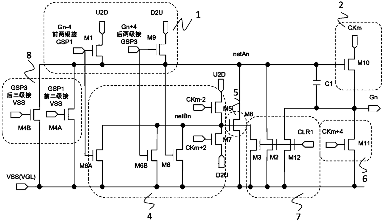
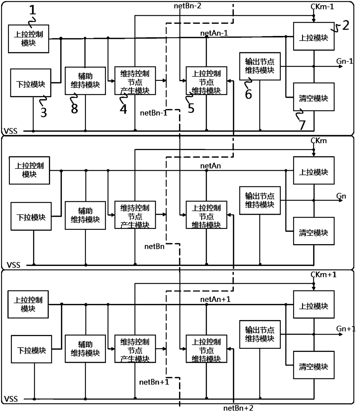
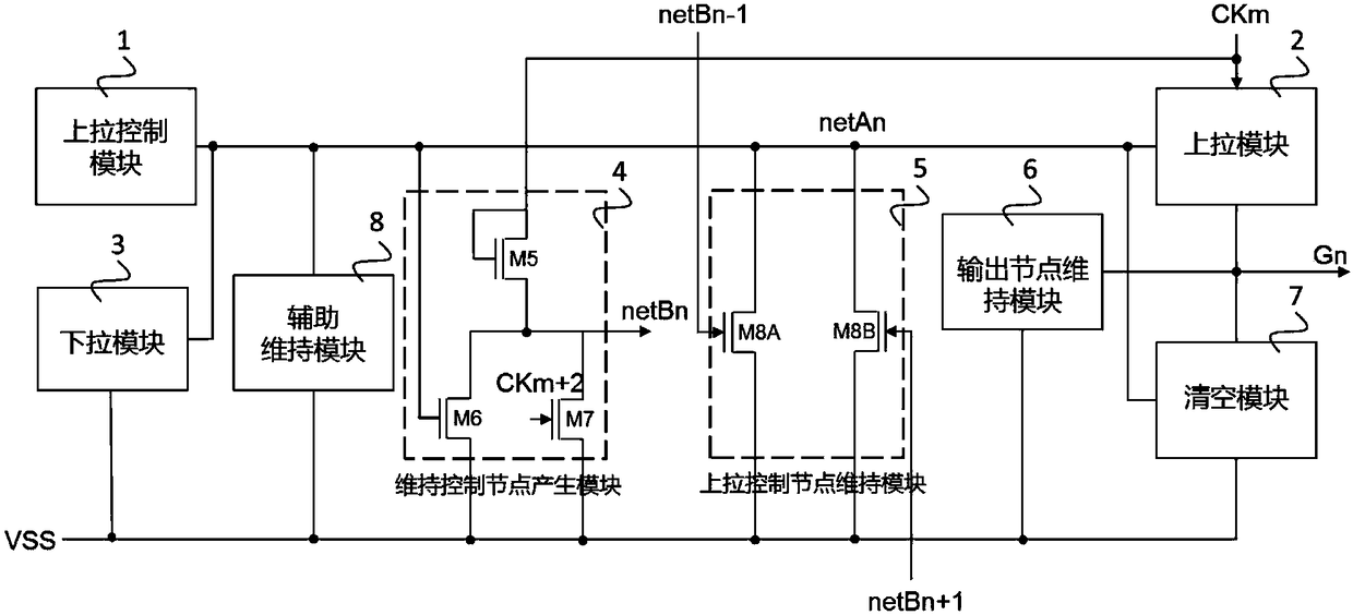
[0075] Such as Figure 5 Shown is a circuit diagram of Embodiment 1 of a gate scanning drive circuit. The nth level drive circuit unit includes a pull-up control module 1, a pull-up module 2, a pull-down module 3, a maintenance control node generation module 4, and a pull-up control node A maintenance module 5 and an output node maintenance module 6 .

[0076] Pull-up control module 1, pull-up module 2, maintenance control node generation module 4 and pull-up control node maintenance module 5 are connected to the pull-up control node netAn; pull-down module 3, maintenance control node generation module 4, pull-up control node maintenance Both the module 5 and the output node maintenance module 6 input low level VSS; the maintenance control node generation module 4 is connected to the maintenance control node netBn; the pull-up module 2 and the output node maintenance module 6 are connected to the scanning signal line of the current stage.

[0077] When 2≦n≦N-1, the maintenanc...

Embodiment 2

[0118] Figure 8 It is a schematic circuit diagram of Embodiment 2 of a gate scanning driving circuit of the present invention. The second embodiment is improved on the basis of the first embodiment, and the specific improvements are as follows:

[0119] The control terminal of the eleventh thin film transistor M11A in the output node maintenance module 6 is connected to the maintenance control node netBn of the driving circuit unit of the current stage, and the two channel terminals of the eleventh thin film transistor M11A are respectively connected to the low level VSS and the scanning signal of the current stage Wire.

Embodiment 3

[0121] Figure 9 It is a schematic circuit diagram of Embodiment 3 of a gate scanning driving circuit of the present invention. The third embodiment is improved on the basis of the first embodiment, and the specific improvements are as follows:

[0122] 1. The output node maintenance module 6 also includes a nineteenth thin film transistor M11B, the control terminal of the nineteenth thin film transistor M11B is connected to the maintenance control node netBn of the drive circuit unit of the current stage, and the two channel terminals of the nineteenth thin film transistor M11B are respectively connected to Low level VSS and the scan signal line of this stage. The eleventh thin film transistor M11A and the sixteenth thin film transistor M11B jointly maintain the output node Gn to enhance the sustaining capability.


PUM


Abstract

The invention discloses a grid scanning drive circuit which comprises N levels of drive circuit units, and N represents a positive integer greater than 3. The n level of drive circuit unit (n represents a positive integer greater than or equivalent to 1 and lower than or equivalent to N) comprises a pull-up control module, a pull-up module, a pull-down module, a maintaining control node generationmodule, a pull-up control mode maintaining module and an output node maintaining module; and when n is greater than or equivalent to 2 and lower than or equivalent to N-1, the maintaining control node generation module of the n level drive circuit unit is connected with the pull-up control mode maintaining module of the n-1 level of drive circuit unit and the pull-up control mode maintaining module of the n+1 level of drive circuit unit, and the pull-up control mode maintaining module of the n level of drive circuit unit is connected with the maintaining control node generation module of then-1 level of drive circuit unit and the maintaining control node generation module of the n+1 level of drive circuit unit.

Description

technical field [0001] The invention relates to the field of liquid crystal display, in particular to a grid scanning driving circuit. Background technique [0002] The gate scanning lines of flat panel displays were generally driven by integrated circuit chips (Gate IC) before, and the integrated gate scanning drive circuit (Gate Driver Monolithic, GDM) is a method that utilizes the existing manufacturing process of thin film transistor array substrates. The technology in which the gate scanning driving circuit is directly built on the array substrate has the functions of reducing cost, reducing process flow, and reducing the width of the panel frame. With the development of products and technologies, flat panel displays have higher and higher requirements for gate scanning driving circuits, one of which is to have forward scanning and reverse scanning functions at the same time. [0003] figure 1 Shown is a schematic circuit diagram of an existing gate scanning drive cir...

Claims


Application Information

Patent Timeline
Patent Type & Authority Applications(China)
IPC IPC(8): G09G3/36
CPCG09G3/3677G09G2310/0283G09G2310/0286G09G2310/08G09G2310/0281
Inventor 黄洪涛邢程
Owner NANJING CEC PANDA LCD TECH
Why Eureka
Try Eureka