Detection system and method for detecting thin film memristive characteristics by utilizing conductive atomic force microscope device

An atomic force microscope and thin film detection technology, applied in the field of microelectronics, can solve the problems of high reset current, device instability and uniformity, and device power consumption, etc., and achieve the effect of increasing current limiting function and convenient detection method.

Inactive Publication Date: 2018-08-03
SUN YAT SEN UNIV
View PDF3 Cites 2 Cited by
  • Summary
  • Abstract
  • Description
  • Claims
  • Application Information

AI Technical Summary

Problems solved by technology

However, RRAM generally has some problems. For example, its microscopic physical mechanism emerges endlessly, and the device I-V characteristic curve will have a high Reset current, which will increase the power consumption of the device.
In addition, problems such as device instability and uniformity need to be solved urgently.

Method used


Image

  • Detection system and method for detecting thin film memristive characteristics by utilizing conductive atomic force microscope device
  • Detection system and method for detecting thin film memristive characteristics by utilizing conductive atomic force microscope device
  • Detection system and method for detecting thin film memristive characteristics by utilizing conductive atomic force microscope device

Examples


Embodiment Construction

[0017] The accompanying drawings are for illustrative purposes only, and should not be construed as limitations on this patent; in order to better illustrate this embodiment, certain components in the accompanying drawings will be omitted, enlarged or reduced, and do not represent the size of the actual product; for those skilled in the art It is understandable that some well-known structures and descriptions thereof may be omitted in the drawings. The positional relationship described in the drawings is for illustrative purposes only, and should not be construed as a limitation on this patent.

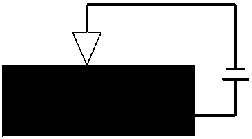
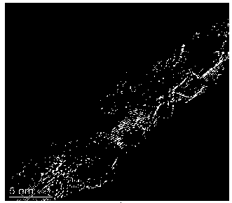
[0018] figure 1 Si in the embodiment of the present invention ++ / Schematic diagram of the structure of a NiO memristor. Including substrate (bottom electrode) Si ++ , a resistive dielectric layer of NiO, and a conductive atomic force microscopy (C-AFM) probe used as the top electrode. Si in the embodiment of the present invention ++ / NiO nano-memristor specific preparation proce...


PUM


Abstract

The invention relates to the technical field of microelectronics, and more particularly relates to a detection system and a detection method for detecting thin film memristive characteristics by utilizing a conductive atomic force microscope device. The detection system is characterized in that the structure of a test sample only comprises a conductive substrate and a variable-resistance dielectric layer. Since the radius of a probe of a conductive atomic force microscope is usually about 20 nm, the detection system can be used for detecting device characteristics under nano-sized microelectrodes, can detect the memristive characteristics under different limited currents through improving the current limiting function of the conductive atomic force microscope, and can detect uniformity ofthin film variable-resistance characteristics by further utilizing the scanning function of the conductive atomic force microscope. The detection method provides a convenient thin film variable-resistance characteristic detection method.

Description

technical field [0001] The invention relates to the technical field of microelectronics, and more specifically, to a detection system and method for detecting the memristive properties of a thin film using a conductive atomic force microscope device. Background technique [0002] The resistive memory device uses the material of the resistive layer to switch the resistive state with the change of the applied electric field, so as to realize the recording and storage of information. Resistive memory devices have the characteristics of simple structure, fast operation speed, and low power consumption, and are expected to greatly increase storage density. However, resistive memory generally has some problems. For example, its microscopic physical mechanism emerges endlessly, and the reset current in the I-V characteristic curve of the device will be high, which will increase the power consumption of the device. In addition, problems such as device instability and uniformity nee...

Claims


Application Information

Patent Timeline
Patent Type & Authority Applications(China)
IPC IPC(8): G01R31/00G01R1/067G01Q60/40
CPCG01Q60/40G01R1/06711G01R31/00
Inventor 裴艳丽李亚储金星
Owner SUN YAT SEN UNIV
Why Eureka
Try Eureka