Etching method, low-temperature polysilicon thin film transistor and AMOLED panel

A low-temperature polysilicon and thin film transistor technology, applied in transistors, electric solid state devices, semiconductor devices, etc., can solve the problems of easy deposition on thin films, black spots on AMOLED panels, and decreased product yield, reducing residual MoClx, improving Product yield, the effect of improving product performance

Active Publication Date: 2018-08-10
TRULY HUIZHOU SMART DISPLAY
View PDF6 Cites 203 Cited by
  • Summary
  • Abstract
  • Description
  • Claims
  • Application Information

AI Technical Summary

Benefits of technology

The technology described in this patented describes an improved way for producing thin films made up of metals such as molybon or tungsten through chemical reactions between gases containing halogen atoms like hydrogen (H2) and oxidizing agents called Sulfursulfur trifluoride (SF6/CF, CF1.5 ) during processing steps used to make these materials. By adding certain types of compounds together with specific amounts of H2/CO/N.3

Problems solved by technology

This patented technical problem addressed in this patents relates to improving the efficiency and resolution of liquid displays made up of organic light emitting diodes (AMLESPDS)). Current technologies have limitations like slow reaction times due to heat processing required but also require expensive equipment and complicated manufacturing techniques. Therefore there are needs for improved ways to improve these issues without compromising their effectiveness.

Method used


Image

  • Etching method, low-temperature polysilicon thin film transistor and AMOLED panel
  • Etching method, low-temperature polysilicon thin film transistor and AMOLED panel
  • Etching method, low-temperature polysilicon thin film transistor and AMOLED panel

Examples


Embodiment Construction

[0030] In order to make the object, technical solution and advantages of the present invention clearer, the present invention will be described in further detail below in conjunction with specific embodiments and with reference to the accompanying drawings.

[0031] Although preferred embodiments of the present disclosure are shown in the drawings, it should be understood that the present disclosure may be embodied in various forms and should not be limited to the embodiments set forth herein. Rather, these embodiments are provided so that this disclosure will be thorough and complete, and will fully convey the scope of the disclosure to those skilled in the art.

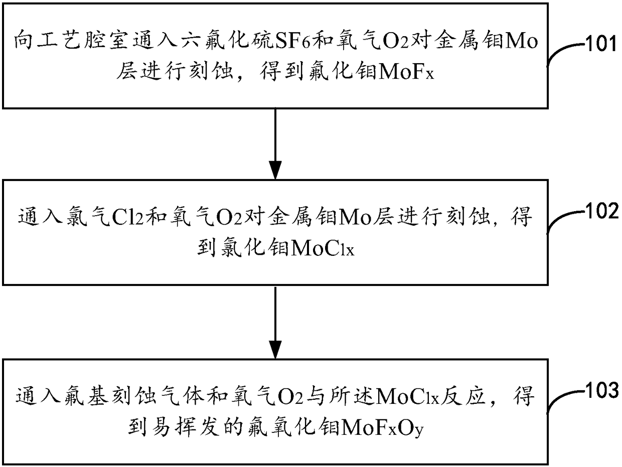
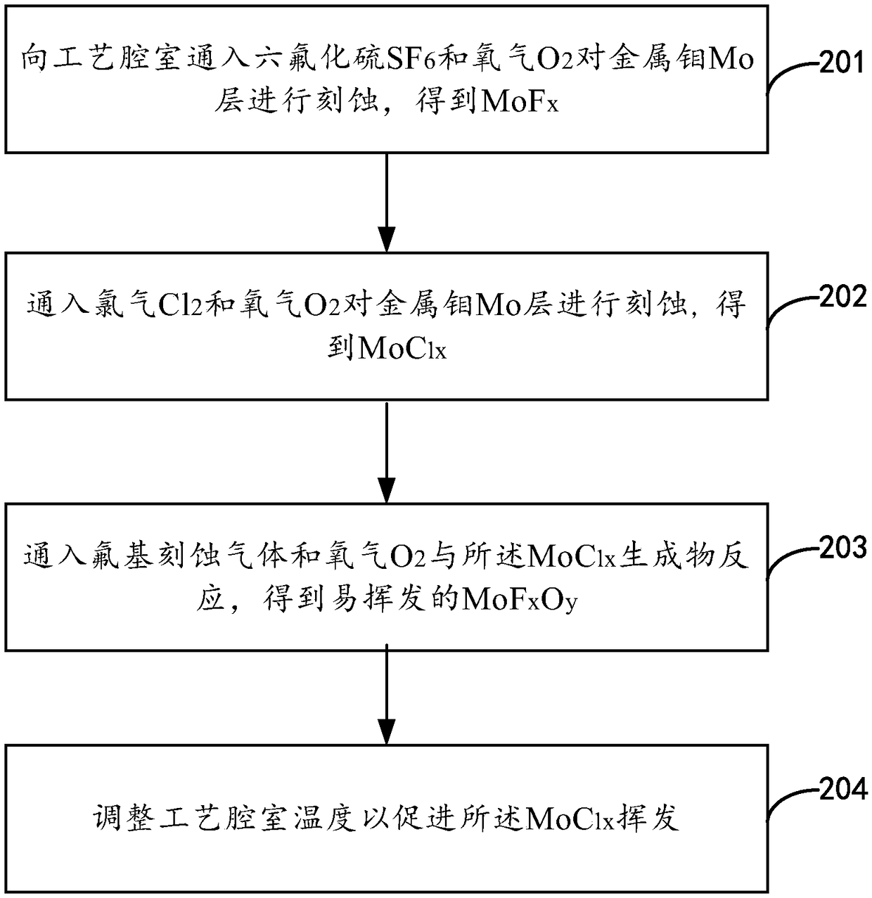
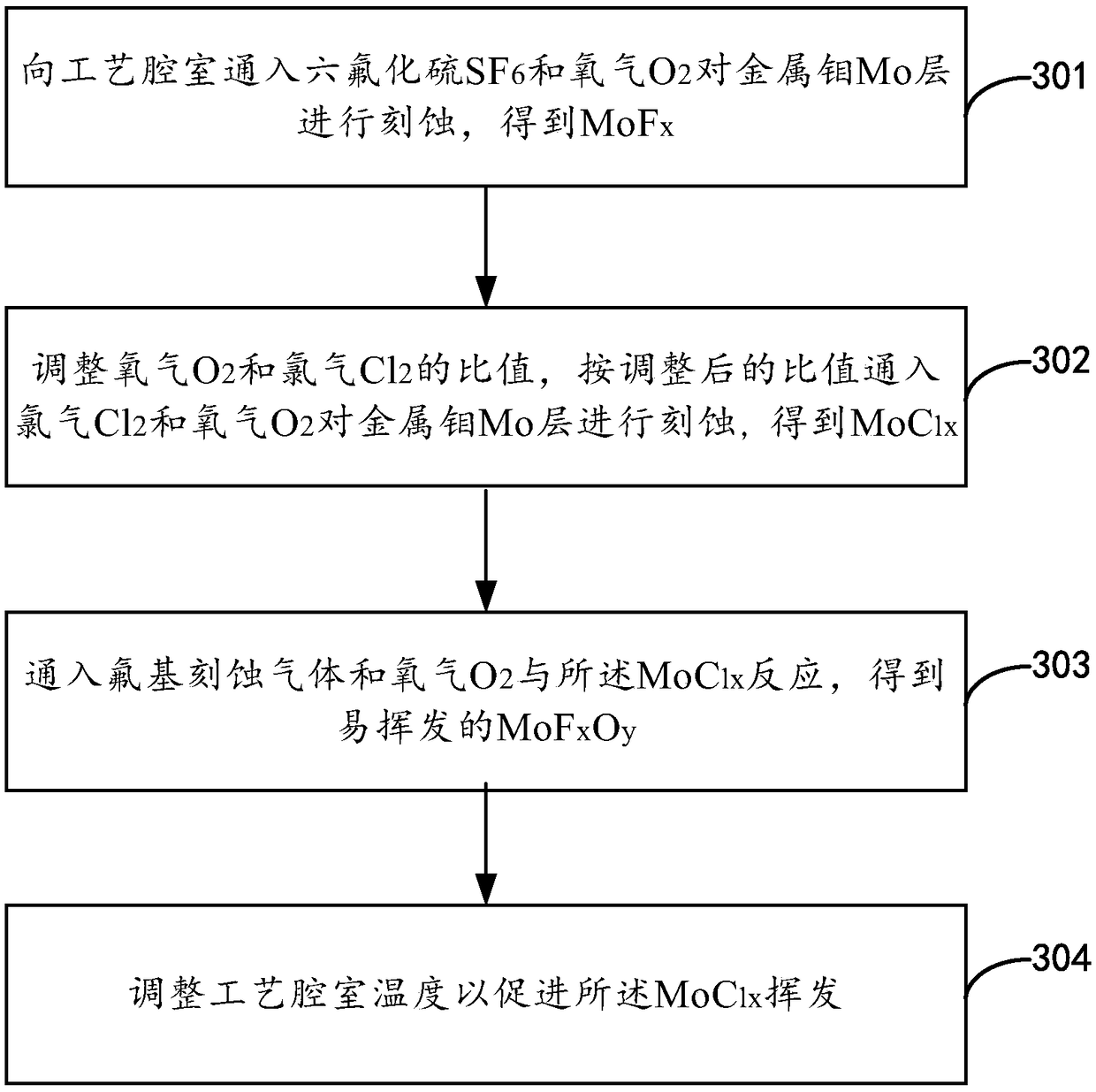
[0032] The invention provides an etching method, which can reduce the residue of dry etching products and solve the abnormal display phenomenon of the AMOLED panel display screen.

[0033] The technical solutions of the embodiments of the present invention will be described in detail below in conjunction with the ac...


PUM


Abstract

The invention discloses an etching method, a low-temperature polysilicon thin film transistor and an AMOLED panel. The etching method comprises the steps of pumping sulfur hexafluoride SF<6> and oxygen O<2> to a process chamber to perform etching on a metal molybdenum Mo layer to obtain molybdenum fluoride MoF<x>; pumping chlorine Cl<2> and oxygen O<2> to perform etching on the metal molybdenum Molayer to obtain molybdenum chloride MoCl<x>; and pumping a fluoro-etching gas and oxygen O<2> to be reacted with MoCl<x> to obtain easily volatile molybdenum oxyfluoride MoF<x>O<y>. By virtue of thescheme provided by the invention, residue of dry etching resultants can be reduced, and the problem of a display abnormal phenomenon of the AMOLED panel is solved.

Description


Claims


Application Information

Patent Timeline
Owner TRULY HUIZHOU SMART DISPLAY
Why Eureka
Try Eureka