Automatic punching molding die of semiconductor product and processing method thereof

A technology for forming molds and semiconductors, applied in the field of semiconductor processing, to achieve the effect of simple molds, simple maintenance equipment, and good production automation

Active Publication Date: 2018-08-21
深圳市华龙精密模具有限公司
View PDF9 Cites 1 Cited by
  • Summary
  • Abstract
  • Description
  • Claims
  • Application Information

AI Technical Summary

Problems solved by technology

[0004] In order to overcome many problems in the existing semiconductor pin processing technology, the invention provides an automatic punching die for semiconductor products and a processing method thereof

Method used


Image

  • Automatic punching molding die of semiconductor product and processing method thereof
  • Automatic punching molding die of semiconductor product and processing method thereof
  • Automatic punching molding die of semiconductor product and processing method thereof

Examples


Embodiment Construction

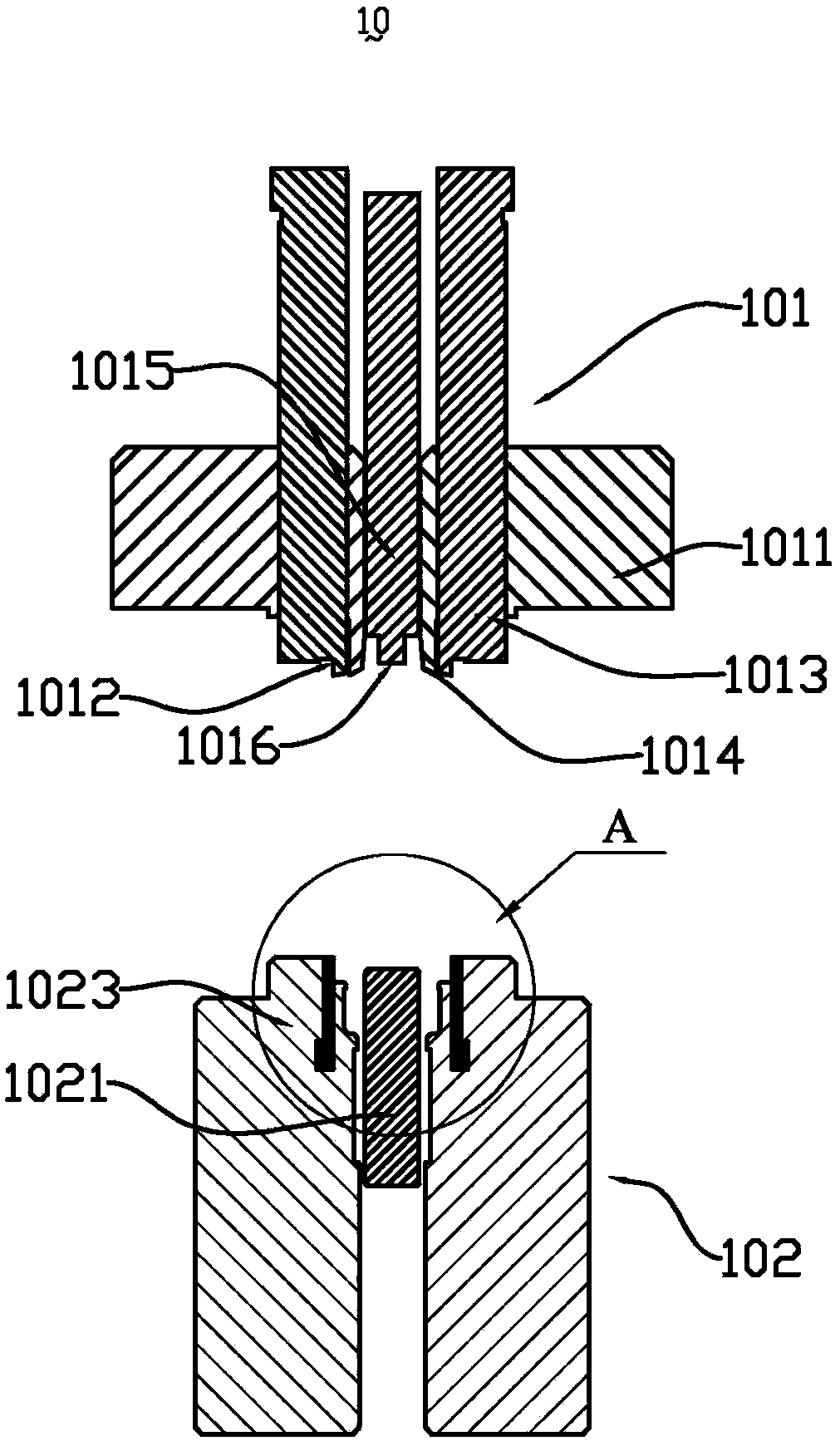
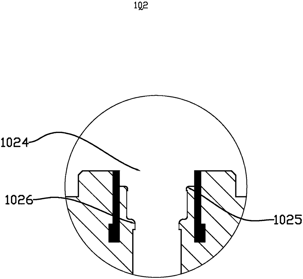
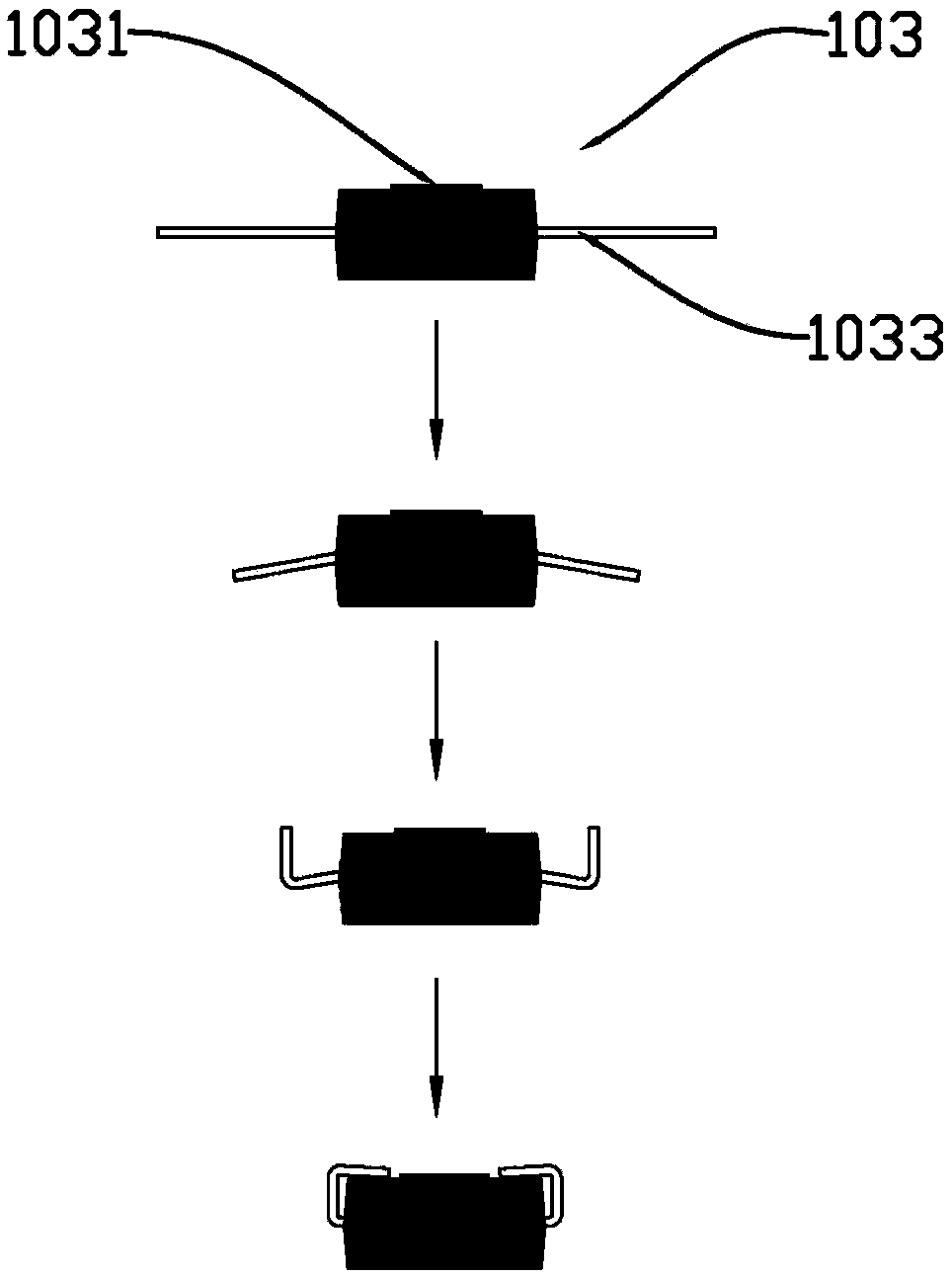
[0026] In order to make the purpose, technical solutions and advantages of the present invention more clear, the present invention will be further described in detail below in conjunction with the accompanying drawings and implementation examples. It should be understood that the specific embodiments described here are only used to explain the present invention, not to limit the present invention.

[0027] It should be noted that when an element is referred to as being “fixed on” or “disposed on” another element, it may be directly on the other element or there may be an intervening element at the same time. When an element is referred to as being "connected to" another element, it can be directly connected to the other element or intervening elements may also be present.

[0028] It should also be noted that the orientation terms such as left, right, up, and down in the embodiments of the present invention are only relative concepts or refer to the normal use state of the pro...


PUM


Abstract

The invention relates to an automatic punching molding die of a semiconductor product. The die comprises an upper die and a lower die, wherein the upper die and the lower die cooperate with each otherto process a to-be-processed workpiece, the upper die comprises a molding mold insert, a male die and a molding pressing block; the male die is embedded in the molding mold insert, and the molding pressing block is embedded in a central trench hole of the molding mold insert; the lower die comprises a female die and a molding floating strip embedded in the female die, the molding floating strip is a strip-shaped structure and can move vertically in the female die. The invention further provides a processing method of the automatic punching molding die of the semiconductor product. Compared with the prior art, the automatic punching molding die of the semiconductor product and the processing method thereof have the advantages that the labor intensity of operating workers can be reduced; the number of the operating workers is reduced, one person can operate a large amount of equipment, thereby improving the production efficiency; and the wearing part cost used by dies can be reduced, thereby improving the product cost performance.

Description

【Technical field】 [0001] The invention relates to the technical field of semiconductor processing, in particular to an automatic punching molding die for semiconductor products formed by wrapping semiconductor pins at one time and a processing method thereof. 【Background technique】 [0002] The pins of SMD products or capacitors in semiconductors are all packaged. At present, the commonly used process in this technical field is stamping production with a manual die. Such a processing method is difficult and dangerous to operate, with low production efficiency and low quality. Another processing technology is the use of automatic punching molds, which require compatibility with two or more stations at the same time. The manufacturing cost of the molds used for processing is very expensive. Due to the collaborative processing of multiple stations, the production operation Very inconvenient. Moreover, when an abnormal shutdown is encountered during production and processing, ...

Claims


Application Information

Patent Timeline
Patent Type & Authority Applications(China)
IPC IPC(8): B21F11/00B21F1/00
CPCB21F1/004B21F11/00
Inventor 何勇赵君龙
Owner 深圳市华龙精密模具有限公司
Why Eureka
Try Eureka