Photonic crystal light emitting device

Inactive Publication Date: 2005-09-22
LUMILEDS
View PDF31 Cites 145 Cited by
  • Summary
  • Abstract
  • Description
  • Claims
  • Application Information

AI Technical Summary

Benefits of technology

[0013] In accordance with embodiments of the device, a photonic crystal structure is formed in an n-type region of a III-nitride semiconductor structure including an active region sandwiched between an n-type region and a p-type region. A reflector is formed on a surface of the p-type region opposite the active region. In some embodiments, the growth substrate on which the n-ty

Problems solved by technology

The extraction efficiency is limited, for example, by the emitted photons suffering multiple total internal reflections at the walls of the high refractive index semiconductor medium.
As a result, the emitted photons do not escape into free space, leading to poor extraction efficiencies, typically less than 30%.
However, none of these geometries can entirely eliminate losses from total internal reflection.
A further source of loss is the reflection caused by the refractive index mismatch between the LED and the surrounding media.
However, the device of U.S. Pat. No. 5,955,749 is not operational and therefore is not a LED.
Also, electrodes are typically thought to reduce the extraction efficiency as they reflect a portion of the emitted photons back into the LED, and absorb another portion of the emitted light.
However, when electrons and holes recombine through intermediate electronic states in the electronic band gap, then the recombination energy is emitted in the form of heat instead of photons, reducing the light emission efficiency of the LED.
However, on the surface of semiconductors typically there are a large number of surface states and defect states, many of them in the electronic band gap.
This surface recombination g

Method used


Image

  • Photonic crystal light emitting device
  • Photonic crystal light emitting device
  • Photonic crystal light emitting device

Examples


Example

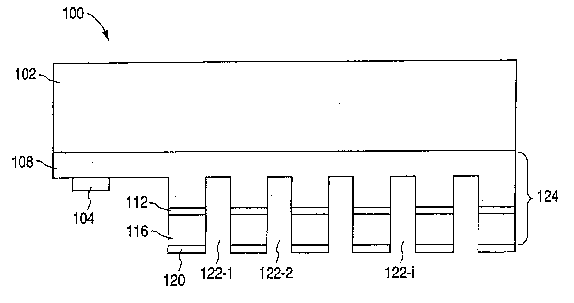
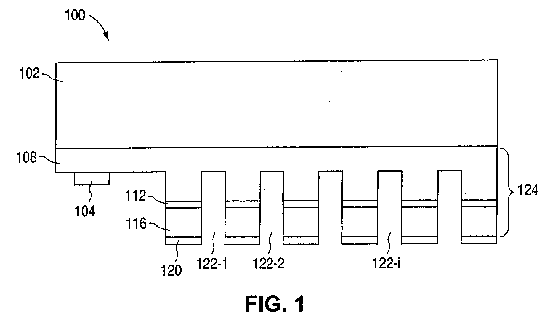
[0027]FIG. 1 illustrates a III-nitride photonic crystal LED (PXLED) 100, described in more detail in application Ser. No. 10 / 059,588, “LED Efficiency Using Photonic Crystal Structure,” filed Jan. 28, 2002 and incorporated herein by reference.

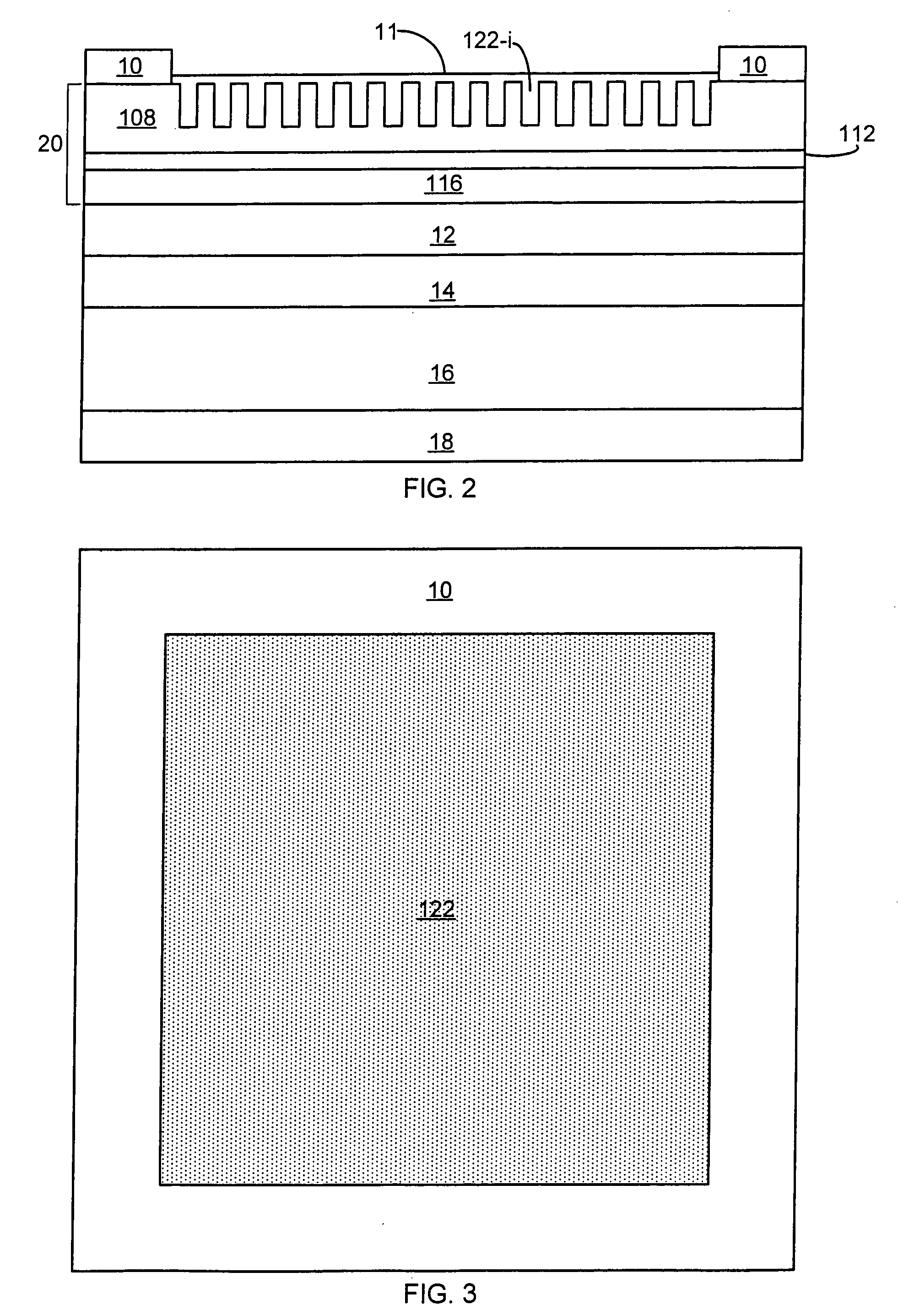
[0028] In PXLED 100 of FIG. 1, an n-type region 108 is formed over host substrate 102 which may be, for example, sapphire, SiC, or GaN; an active region 112 is formed over n-type region 108; and a p-type region 116 is formed over active region 112. Each of regions 108, 112, and 116 may be a single layer or multiple layers of the same or different composition, thickness, or dopant concentration. A portion of p-type region 116 and active region 112 are etched away to expose a portion of n-type region 108, then a p-contact 120 is formed on p-type region 116 and an n-contact 104 is formed on the exposed portion of n-type region 108.

[0029] Active region 112 includes a junction region where electrons from n-type region 108 combine with holes of p-ty...


PUM


Abstract

A photonic crystal structure is formed in an n-type region of a III-nitride semiconductor structure including an active region sandwiched between an n-type region and a p-type region. A reflector is formed on a surface of the p-type region opposite the active region. In some embodiments, the growth substrate on which the n-type region, active region, and p-type region are grown is removed, in order to facilitate forming the photonic crystal in an an-type region of the device, and to facilitate forming the reflector on a surface of the p-type region underlying the photonic crystal. The photonic crystal and reflector form a resonant cavity, which may allow control of light emitted by the active region.

Description

BACKGROUND [0001] 1. Field of Invention [0002] The present invention relates to semiconductor light emitting devices including photonic crystal structures. [0003] 2. Description of Related Art [0004] Light emitting diodes (“LEDs”) are technologically and economically advantageous solid state light sources. LEDs are capable of reliably providing light with high brightness, hence in the past decades they have come to play a critical role in numerous applications, including flat-panel displays, traffic lights, and optical communications. An LED includes a forward biased p-n junction. When driven by a current, electrons and holes are injected into the junction region, where they recombine and release their energy by emitting photons. The quality of an LED can be characterized, for example, by its extraction efficiency, which measures the intensity of the emitted light for a given number of photons generated within the LED chip. The extraction efficiency is limited, for example, by the e...

Claims


Application Information

Patent Timeline
IPC IPC(8): H01L33/00H01L33/10H01L33/20H01L33/38H01L33/62
CPCH01L33/0079H01L33/10H01L33/22H01L33/382H01L33/62H01L2924/0002H01L2933/0083H01L2924/00H01L33/0093
Inventor WIERER, JONATHAN J. JR.KRAMES, MICHAEL R.EPLER, JOHN E.
Owner LUMILEDS
Why Eureka
Try Eureka