Manufacture method of optical voltage/electric field sensor wafer capable of suppressing piezoelectric resonance

An electric field sensor, optical voltage technology, applied in the manufacture/assembly of piezoelectric/electrostrictive devices, piezoelectric/electrostrictive/magnetostrictive devices, circuits, etc.

Inactive Publication Date: 2018-08-21
TSINGHUA UNIV
View PDF4 Cites 1 Cited by
  • Summary
  • Abstract
  • Description
  • Claims
  • Application Information

AI Technical Summary

Problems solved by technology

Currently, there are no related reports

Method used


Image

  • Manufacture method of optical voltage/electric field sensor wafer capable of suppressing piezoelectric resonance
  • Manufacture method of optical voltage/electric field sensor wafer capable of suppressing piezoelectric resonance
  • Manufacture method of optical voltage/electric field sensor wafer capable of suppressing piezoelectric resonance

Examples


Embodiment 1

[0047] Embodiment 1: the first kind of scheme of the present invention is applied to the making of the common path interference sensor chip that can suppress piezoelectric resonance under the lightning wave condition, and the common path interference sensor that is made of this chip is used under the lightning wave condition in the power grid line, The frequency of the electric field is f min ~ f max (The present embodiment is 50Hz~1MHz) voltage / electric field measurement, the width direction of wafer is perpendicular to light source transmission direction; The method comprises the following steps:

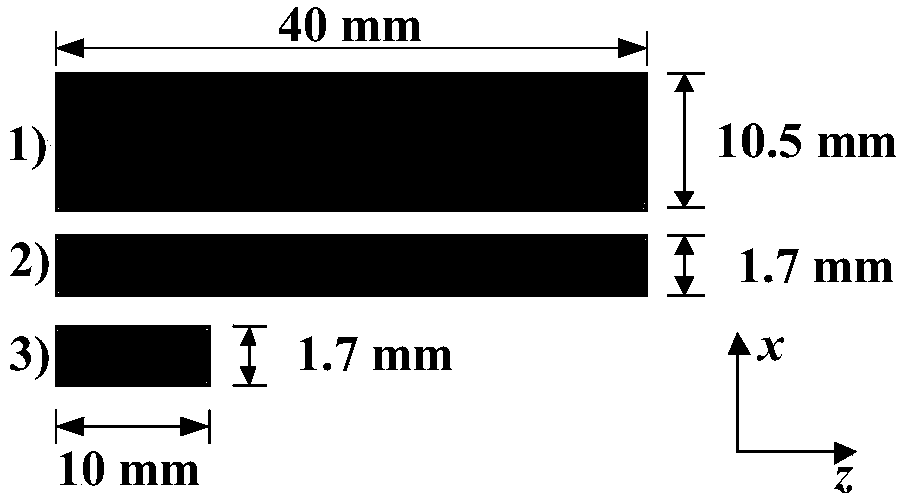
[0048] S1: Select a parallelogram test wafer with the same material as the wafer to be produced, and the width of the test wafer is W 0 (the present embodiment is 5.6mm);

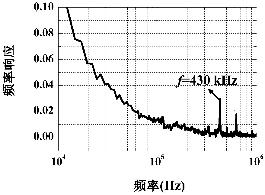
[0049] S2: The frequency range of the electric field on the test wafer is f min ~ f max The frequency response test of the electric field, measured the piezoelectric resonance fundamental frequency of the t...

Embodiment 2

[0054] Embodiment 2: The second kind of scheme of the present invention is applied to the making of the common path interference sensor chip that can suppress piezoelectric resonance under the lightning wave condition, and the common path interference sensor that this chip forms is used for under the lightning wave condition in the power grid line, electric field frequency is f min ~ f max (The present embodiment is 50Hz~1MHz) voltage / electric field measurement, the width direction of wafer is perpendicular to light source transmission direction; The method comprises the following steps:

[0055] S1: Select a parallelogram test wafer with the same material as the wafer to be produced, and the width of the test wafer is W 0 (the present embodiment is 5.6mm);

[0056] S2: The frequency range of the electric field on the test wafer is f min ~ f max According to the electric field frequency response test, the piezoelectric resonance fundamental frequency of the wafer is f 0 (...


PUM


Abstract

The invention discloses a manufacture method of an optical voltage/electric field sensor wafer capable of suppressing piezoelectric resonance and belongs to the optical voltage/electric field sensor technical field. According to one embodiment of the invention, a value in a set range is selected for the width of the wafer, and therefore, the resonant fundamental frequency of an optical voltage/electric field sensor composed of the wafer can be transferred to be a frequency outside a frequency range required to be measured; according to another embodiment of the invention, the width of the wafer is set to change gradually, so that the resonant energy of the optical voltage/electric field sensor composed of the wafer can be dispersed. The optical voltage/electric field sensor composed of thewafer prepared by the method of the invention effectively suppresses a piezoelectric resonance phenomenon under a condition of a set electric field frequency. The method is simple in operation and easy to implement.

Description

technical field [0001] The invention relates to the technical field of optical voltage / electric field sensors, in particular to a manufacturing method of an optical voltage / electric field sensor capable of suppressing piezoelectric resonance. Background technique [0002] Due to its small size, high frequency response, no electromagnetic compatibility problem, and little interference to the original field, the optical voltage and electric field sensor has been widely valued in the field of voltage and electric field measurement. [0003] Most of the electro-optic chips used in optical voltage electric field sensors are also piezoelectric chips, and there is piezoelectric resonance phenomenon. , Tokuda M. Improvement of frequency characteristics of electric field sensoruring Mach-Zehnder interferometer. Electron Comm Jap, 2000, 83:699-706.). However, this characteristic leads to large errors in the measurement of voltage and electric field signals of certain specific frequen...

Claims


Application Information

Patent Timeline
Patent Type & Authority Applications(China)
IPC IPC(8): H01L41/33H01L41/338
CPCH10N30/08H10N30/088
Inventor 曾嵘庄池杰汪海余占清王博
Owner TSINGHUA UNIV
Why Eureka
Try Eureka