Magnetron sputtering cavity and magnetron sputtering device
A magnetron sputtering and chamber technology, applied in the field of magnetron sputtering, can solve the problems of poor film uniformity, cumbersome process, unsuitable for large-size wafer production, etc., and achieves good film thickness uniformity and improves uniformity. Effect
- Summary
- Abstract
- Description
- Claims
- Application Information
AI Technical Summary
Problems solved by technology
Method used
Image

Examples
Embodiment 1
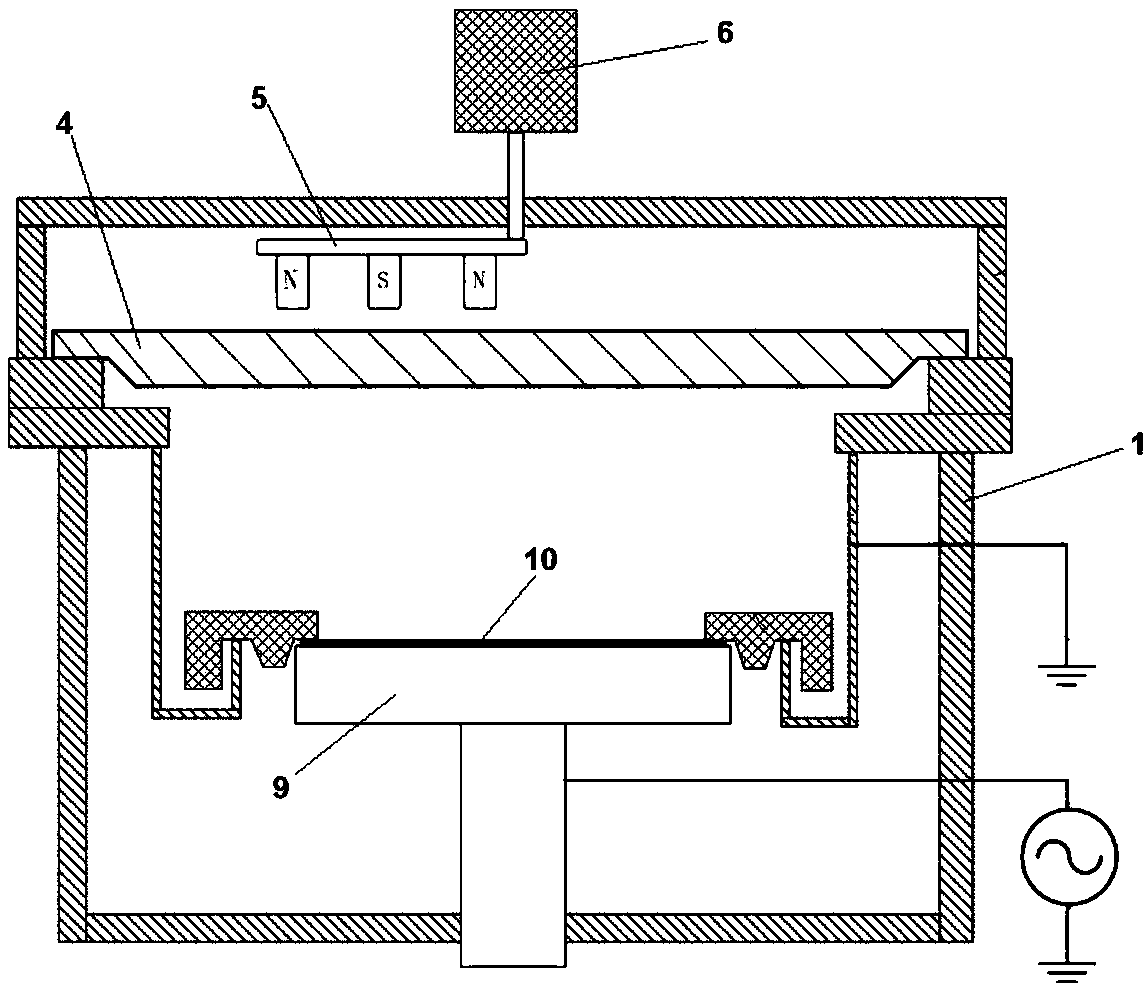
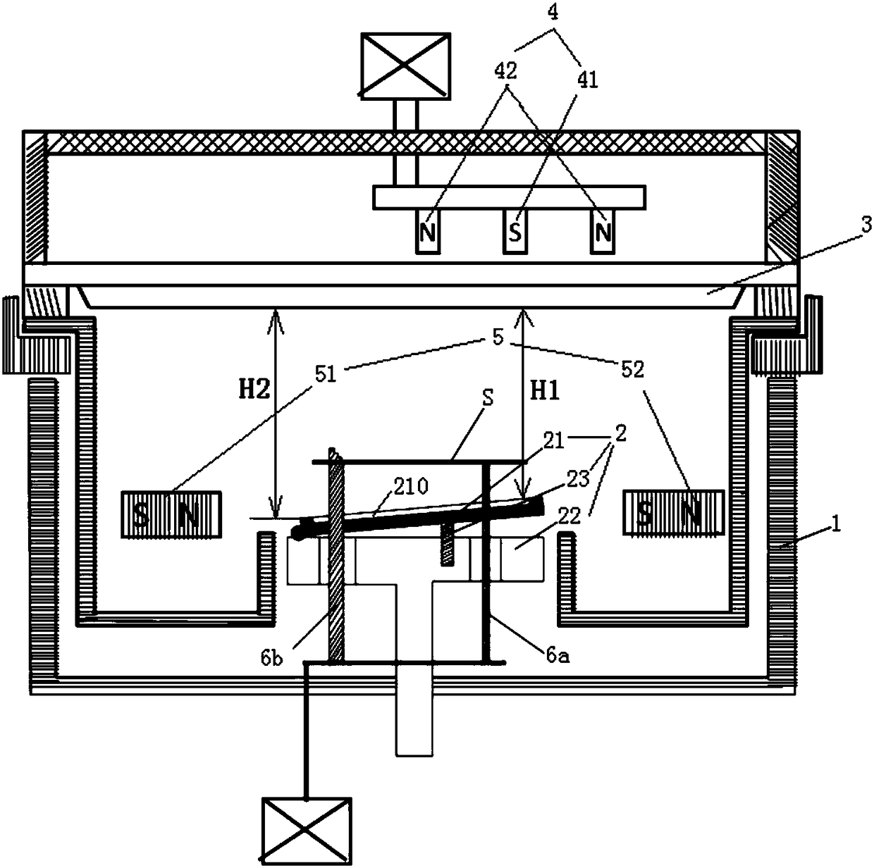
[0024] figure 2 The structural representation of the magnetron sputtering chamber that the embodiment of the present invention provides; Please refer to figure 2 , The magnetron sputtering chamber provided by the embodiment of the present invention includes a chamber body 1, and a base 2 is arranged in the chamber body 1; The target position of 3; a magnetron 4 is arranged above the target 3, and the magnetron 4 includes an inner magnetic pole 41 and an outer magnetic pole 42 of opposite polarity, and a magnetic field track is formed between the inner magnetic pole 41 and the outer magnetic pole 42.
[0025] The upper surface of the pedestal 2 for carrying the substrate is arranged obliquely, during the process (or in other words, when the substrate is on the pedestal 2, it is used to make the thinner substrate area on the substrate relative to the deposition thickness. Thicker substrate area and target position ( figure 2 The distance between the position where the targe...
Embodiment 2
[0038] The embodiment of the present invention also provides a magnetron sputtering device, including a magnetron sputtering chamber, and the magnetron sputtering chamber adopts the magnetron sputtering chamber provided in Embodiment 1 of the present invention.
[0039] The magnetron sputtering equipment provided by the embodiment of the present invention includes the magnetron sputtering chamber provided by the above-mentioned embodiment 1 of the present invention, therefore, an in-plane anisotropic magnetic film with better film thickness uniformity can be obtained.
PUM
 Abstract
Description
Claims
Application Information
 - Generate Ideas
- Intellectual Property
- Life Sciences
- Materials
- Tech Scout
- Unparalleled Data Quality
- Higher Quality Content
- 60% Fewer Hallucinations
Browse by: Latest US Patents, China's latest patents, Technical Efficacy Thesaurus, Application Domain, Technology Topic, Popular Technical Reports.
© 2025 PatSnap. All rights reserved.Legal|Privacy policy|Modern Slavery Act Transparency Statement|Sitemap|About US| Contact US: help@patsnap.com