Manufacturing technology of semiconductor diode

A manufacturing process and diode technology, which is applied in semiconductor/solid-state device manufacturing, semiconductor devices, electrical components, etc., can solve the problems of easy wrinkling and cracking of the glue layer, so that it is not easy to wrinkle and break, save the cleaning process, The effect of saving resources

Active Publication Date: 2018-08-31
上海朋熙半导体有限公司
View PDF5 Cites 2 Cited by
  • Summary
  • Abstract
  • Description
  • Claims
  • Application Information

AI Technical Summary

Problems solved by technology

The invention improves the diode production and manufacturing process through the diode pin forming equipment, and solves the problem that the glue layer is easy to wrinkle or the glue layer is easy to break when the glued diode pin is bent and formed.

Method used


Image

  • Manufacturing technology of semiconductor diode
  • Manufacturing technology of semiconductor diode
  • Manufacturing technology of semiconductor diode

Examples


Embodiment Construction

[0035] In order to make the technical means, creative features, goals and effects achieved by the present invention easy to understand, the present invention will be further described below in conjunction with specific embodiments.

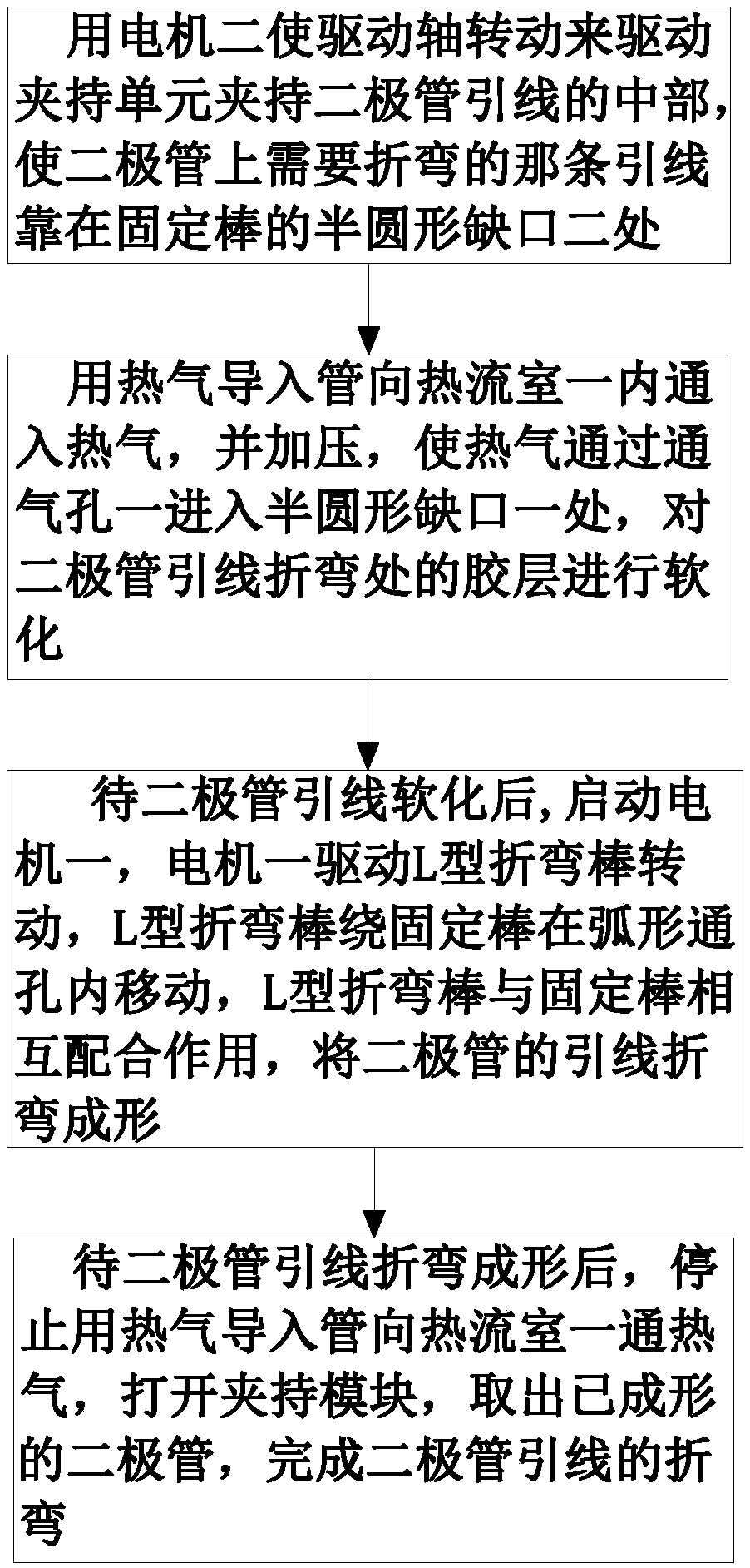
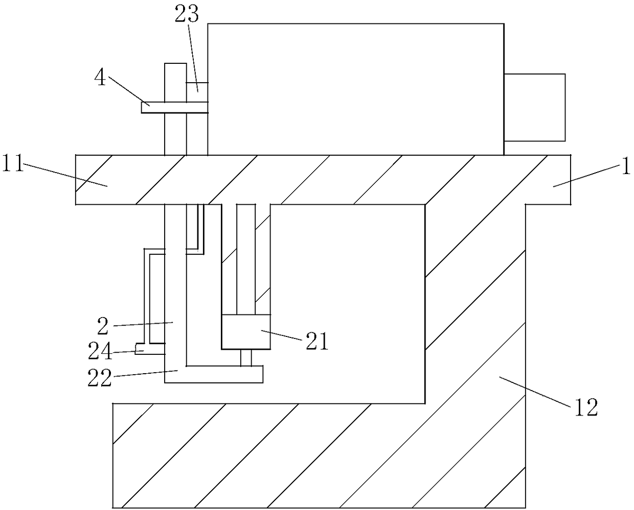
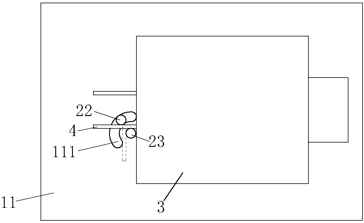
[0036] like Figure 1-8 As shown, a semiconductor diode production and manufacturing process is manufactured using the following process steps:

[0037] Step 1: pickling; place the diode chip in a mixed acid solution of sulfuric acid and phosphoric acid for acid etching, and the volume ratio of sulfuric acid and phosphoric acid is 1:2, the etching time is 10-15min, and the acid temperature is controlled between 1-5°C between;

[0038] Step 2: electroplating; after the pickling process in step 1 is completed, the pickled diode chip is electroplated to form a metal protection layer on the surface of the diode chip, the thickness of the coating is 3-5 μm, and the coating metal is tin;

[0039] Step 3: Welding; after the electroplating process of st...


PUM


Abstract

The invention belongs to the technical field of manufacturing of diodes, and particularly discloses a manufacturing technology of a semiconductor diode. The manufacturing technology comprises the steps of acid pickling, electroplating, welding, insulation protection, pin bending, aftertreatment and the like. Diode pin forming equipment used in the pin bending procedure comprises a mounting shelf,a bending module and a clamping module, and the mounting shelf comprises a workbench and a supporting shelf; the supporting shelf is located at the lower end of the workbench; an arc through hole is formed in the workbench and located in the bending module; the clamping module is located on a workbench top of the workbench, detachably connected with the workbench, and used for clamping pins of thediode; the bending module is located at the end of the clamping module, and used for bending the pins of the diode. By means of the manufacturing technology of the semiconductor diode, the manufacturing technology of the diode is improved through the diode pin forming equipment, so that the bending mode of the pins of the diode is simpler, the bending efficiency of the pins of the diode is improved, and the quality of the diode is improved.

Description

technical field [0001] The invention belongs to the technical field of diode production and manufacturing, in particular to a semiconductor diode production and manufacturing process. Background technique [0002] Diode is one of the most commonly used electronic components. The biggest characteristic is unidirectional conduction, that is, current can only flow from one direction of the diode. The function of the diode is a rectifier circuit, a detection circuit, a voltage regulator circuit, and various modulation circuits Mainly composed of diodes; [0003] At present, diodes are soldered with chips, solder and leads at high temperature, and then acid-treated on the surface of the chips. However, during the pickling process, metal impurities in the solder and leads will react with the acid, affecting the corrosion rate of the chips. At the same time, The metal ions generated by the reaction of these metals with the acid will adhere to the surface of the chip, and a large a...

Claims


Application Information

Patent Timeline
Patent Type & Authority Applications(China)
IPC IPC(8): H01L21/329
CPCH01L29/6609
Inventor 陈欣洁王勇
Owner 上海朋熙半导体有限公司
Why Eureka
Try Eureka