Sub-wavelength layered three-dimensional broadband absorbing structure based on a loss type frequency selective surface

A frequency-selective surface, sub-wavelength technology, applied in the field of electromagnetic fields and microwaves, can solve the problems of difficult low-frequency absorption performance, complex preparation process, poor absorption effect, etc., and achieve the effect of light weight, thin thickness, and wide operating frequency band.

Active Publication Date: 2018-09-04
NANJING UNIV
View PDF8 Cites 12 Cited by
  • Summary
  • Abstract
  • Description
  • Claims
  • Application Information

AI Technical Summary

Problems solved by technology

Traditional absorbing materials, such as Jaumann absorbers and Salisbury screens, paste lossy films on the medium with a thickness of 1/4 wavelength from the back metal backplane, forming standing waves so that energy is confined in the medium, and the lossy film passes through the surface. The loss of the film and the medium achieves wave absorption, but its disadvantage is that it is thicker
Today's wave-absorbing materials mainly realize the characteristics that natural materials do not have by designing artificial electromagnetic metamaterials. For example, using metasurfaces to design wave-absorbing structures with a very thin thickness can achieve perfect absorption of electromagnetic waves at a certain frequency point. But the disadvantage is that the absorbing frequency band is relatively narrow
[0003] Traditional absorbing materials and new sup...

Method used


Image

  • Sub-wavelength layered three-dimensional broadband absorbing structure based on a loss type frequency selective surface
  • Sub-wavelength layered three-dimensional broadband absorbing structure based on a loss type frequency selective surface
  • Sub-wavelength layered three-dimensional broadband absorbing structure based on a loss type frequency selective surface

Examples


Embodiment Construction

[0020] Below in conjunction with accompanying drawing and specific embodiment, further illustrate the present invention, should be understood that these embodiments are only for illustrating the present invention and are not intended to limit the scope of the present invention, after having read the present invention, those skilled in the art will understand various aspects of the present invention Modifications in equivalent forms all fall within the scope defined by the appended claims of this application.

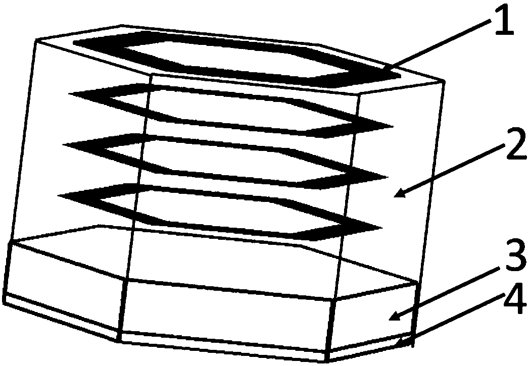
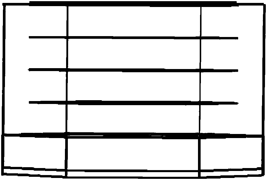
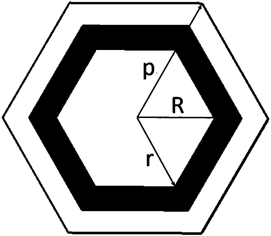
[0021] Figure 1-Figure 4 A schematic diagram showing a sub-wavelength layered three-dimensional broadband absorbing structure based on a lossy frequency selective surface according to an embodiment of the present invention. In this embodiment, the broadband absorbing structure is a periodic array structure composed of multiple structural units, where each structural unit, such as figure 1 , 2 As shown, it includes four ring-shaped loss-type frequency selective surface...


PUM

PropertyMeasurementUnit
Conductivityaaaaaaaaaa
The inside diameter ofaaaaaaaaaa
Thicknessaaaaaaaaaa

Abstract

The invention discloses a sub-wavelength layered three-dimensional broadband absorbing structure based on a loss type frequency selective surface. The sub-wavelength layered three-dimensional broadband absorbing structure is a periodic array structure formed by a plurality of structural units. Each structural unit consists of four annular frequency selective surfaces a dielectric layer serving asa supporting layer, a ferrite layer arranged at the lower surface of the dielectric layer, and a metal backing plate arranged at the lower surface of the ferrite layer; and the four annular frequencyselective surfaces are uniformly distributed in the dielectric layer in the vertical direction. The ferrite layer uses ferrite with a working frequency lower than 2 GHz; and the annular frequency selective surfaces are made of conductive materials with the electric conductivity of 100-200 S/m. According to the invention, with the sub-wavelength layered three-dimensional broadband absorbing structure, the wide-band absorption of spatial electromagnetic waves is realized. The sub-wavelength layered three-dimensional broadband absorbing structure has advantages of being insensitive to electromagnetic wave polarization, having the light weight, having a simple structure, being easy to process, having the low cost, having the wide working frequency band and having the relative thin thickness.

Description

technical field [0001] The invention belongs to the field of electromagnetic field and microwave technology, and in particular relates to a sub-wavelength layered three-dimensional broadband wave-absorbing structure based on a lossy frequency selective surface. Background technique [0002] The absorbing material can realize the absorption of the incident electromagnetic wave and achieve the effect of reducing the reflection. Traditional absorbing materials, such as Jaumann absorbers and Salisbury screens, paste lossy films on the medium with a thickness of 1 / 4 wavelength from the back metal backplane, forming standing waves so that energy is confined in the medium, and the lossy film passes through the surface. The loss of the film and the medium achieves wave absorption, but its disadvantage is that it is thicker. Today's wave-absorbing materials mainly realize the characteristics that natural materials do not have by designing artificial electromagnetic metamaterials. Fo...

Claims


Application Information

Patent Timeline
IPC IPC(8): H01Q17/00
CPCH01Q17/008
Inventor 孟凡广伍瑞新
Owner NANJING UNIV
Why Eureka
Try Eureka