Manufacturing method of shallow trench insulation structure

A shallow trench insulation and manufacturing method technology, applied in semiconductor/solid-state device manufacturing, electrical components, circuits, etc., can solve problems affecting chemical mechanical patterns, poor control, poor disc defects, etc.

Active Publication Date: 2018-09-11
SHANGHAI HUALI INTEGRATED CIRCUTE MFG CO LTD
View PDF3 Cites 0 Cited by
  • Summary
  • Abstract
  • Description
  • Claims
  • Application Information

AI Technical Summary

Problems solved by technology

Usually the depth of the shallow groove 104 is more than Above, this makes the depth loading performance corresponding to the shallow trenches 104 of different widths after etching not good; further, the overburden loading formed on the surface after the insulating material 105 is filled is also not good, and finally affects the pattern loading of chemical mechanical polishing.
The common insulating material on the market is usually silicon dioxide, and the slurry properties of this material tend to have poor local morphology and cause poor dishing defects
In the above three conditions of poor loading and dish-shaped defects, the control of the step height (STI step height wafer to wafer) of the shallow trench insulation structure between the wafers will be relatively poor, and it is necessary to use advanced batch processes Control (auto-process control, APC) operation, which is time-consuming and results in poor machine production efficiency

Method used


Image

  • Manufacturing method of shallow trench insulation structure
  • Manufacturing method of shallow trench insulation structure
  • Manufacturing method of shallow trench insulation structure

Examples


Embodiment Construction

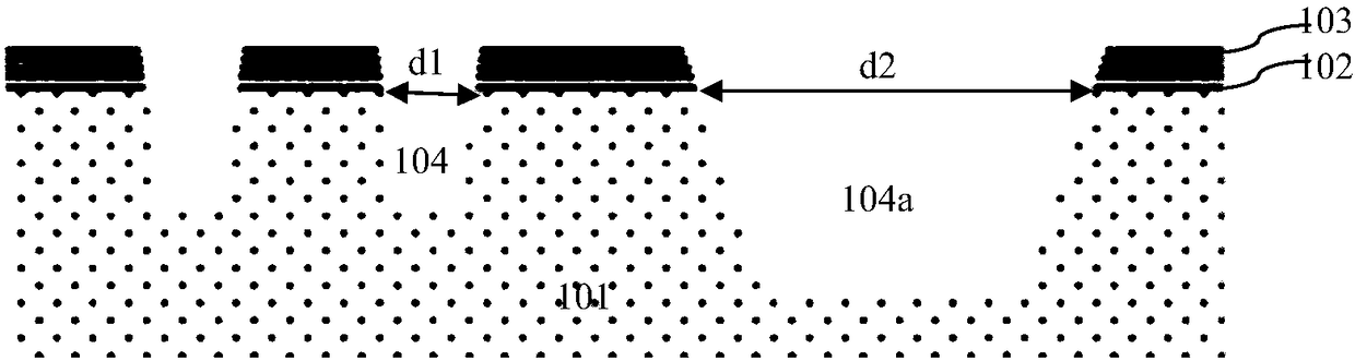
[0035] Such as figure 2 As shown, it is a flow chart of the manufacturing method of the shallow trench isolation structure 7 according to the embodiment of the present invention; Figure 3A to Figure 3F As shown, it is a device structure diagram in each step of the method of the embodiment of the present invention. The manufacturing method of the shallow trench insulation structure 7 of the embodiment of the present invention includes the following steps:

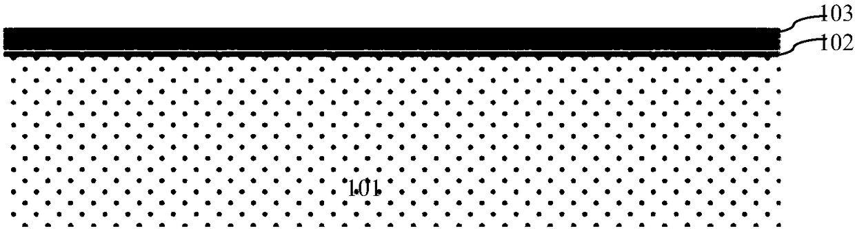
[0036] Step 1, such as Figure 3A As shown, a semiconductor substrate 1 is provided. In the embodiment of the present invention, the semiconductor substrate 1 is a silicon substrate.

[0037] Such as Figure 3B As shown, a hard mask layer is formed on the semiconductor substrate 1 .

[0038]In the embodiment of the present invention, the hard mask layer is formed by stacking the fourth oxide layer 2 and the third nitride layer 3 . The chemical mechanical polishing in the subsequent step 4 uses the third nitride layer ...


PUM


Abstract

The invention discloses a manufacturing method of a shallow trench insulation structure. The manufacturing method comprises the following steps: step 1, forming a hard mask layer on a semiconductor substrate and forming a shallow trench; step 2, forming a first insulating layer on the bottom surface and the side surface of a shallow trench and the surface of the hard mask layer outside the shallowtrench; step 3, forming a second insulating layer to completely fill the shallow trench and extend out of the shallow trench; step 4, performing chemical mechanical grinding on the second insulatinglayer and the first insulating layer by using the hard mask layer as a stop layer, and forming a shallow trench insulation structure formed by superposing the first insulating layer and the second insulating layer which are filled in the shallow trench. According to the invention, the flattening effect of the whole substrate surface can be improved, the disc-shaped defects at the top of the shallow trench insulation structure can be reduced or eliminated, and the CMP efficiency can be improved.

Description

technical field [0001] The invention relates to a method for manufacturing a semiconductor integrated circuit, in particular to a method for manufacturing a shallow trench insulation structure (STI). Background technique [0002] Shallow trench isolation (STI) is used to isolate active areas such as Figure 1A to Figure 1E Shown is a device structure diagram in each step of the existing shallow trench isolation structure manufacturing method; the existing shallow trench isolation structure manufacturing method includes the following steps: [0003] Step 1, such as Figure 1A As shown, a semiconductor substrate such as a silicon substrate 101 is provided. [0004] Such as Figure 1B As shown, a pad oxide layer (Pad Oxide) 102 and a pad nitride layer (Pad SiN) 103 are sequentially formed on the surface of a semiconductor substrate 101, and the pad oxide layer 102 and the pad nitride layer 103 are stacked to form a hard layer. mask layer. In the field of semiconductor integ...

Claims


Application Information

Patent Timeline
IPC IPC(8): H01L21/762
CPCH01L21/76229
Inventor 李昱廷刘怡良龚昌鸿
Owner SHANGHAI HUALI INTEGRATED CIRCUTE MFG CO LTD
Why Eureka
Try Eureka