

Interlayer film manufacturing method
A manufacturing method and interlayer film technology, which are applied in semiconductor/solid-state device manufacturing, electrical components, circuits, etc., can solve problems affecting device performance, metal residues, and exposure of the embedded germanium-silicon layer 108, so as to avoid electrical performance, No metal residue effect
- Summary
- Abstract
- Description
- Claims
- Application Information
AI Technical Summary
Problems solved by technology
Method used
Image

Examples
Embodiment Construction
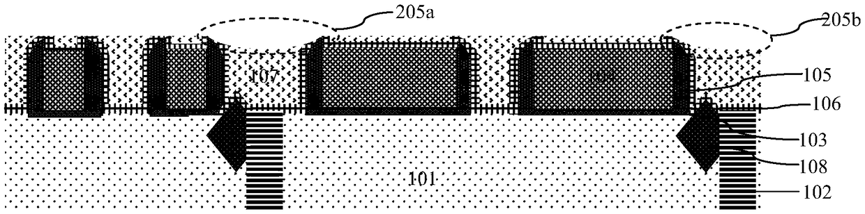
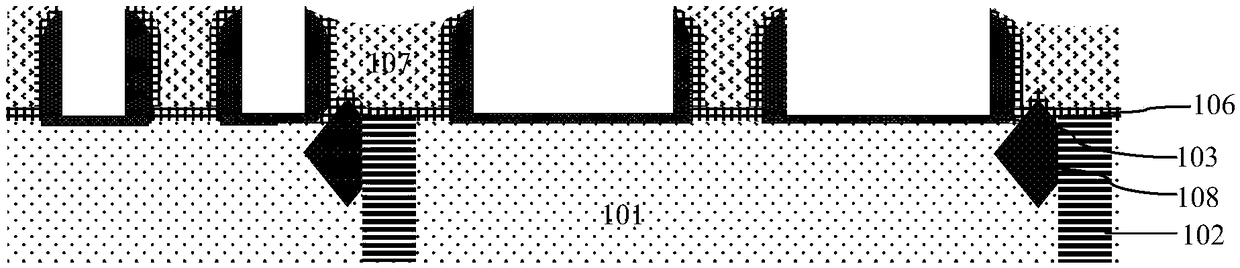
[0050] Such as figure 2 Shown is the flowchart of the manufacturing method of the interlayer film 7 of the embodiment of the present invention; Figure 3A to Figure 3C As shown, it is a device structure diagram in each step of the method of the embodiment of the present invention. The method for manufacturing the interlayer film 7 of the embodiment of the present invention includes the following steps:
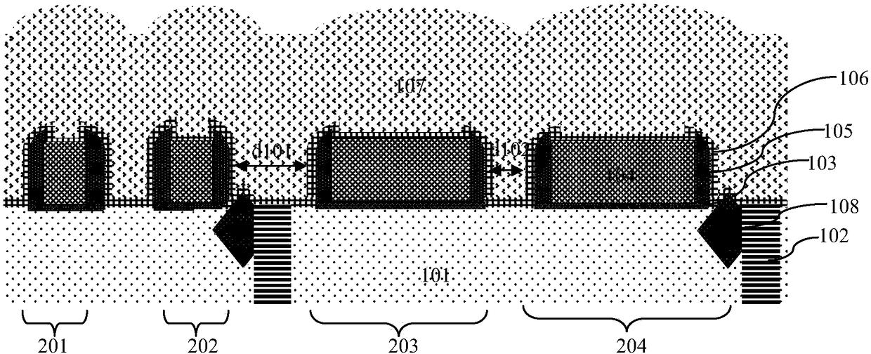
[0051] Step 1, such as Figure 3A As shown, a semiconductor substrate 1 is provided, on which pattern structures of semiconductor devices are formed, and the regions between the pattern structures are pattern spacers.
[0052] In the embodiment of the present invention, the semiconductor substrate 1 is a silicon substrate.
[0053] The semiconductor device is a MOS transistor with HKMG. The interlayer film 7 is the zeroth interlayer film 7 . Usually, the semiconductor device will form multiple layers of metal, wherein the metal layers of each layer need to be isolated by ...
PUM
 Abstract
Description
Claims
Application Information