A kind of manufacturing method of ldmos device

A manufacturing method and device technology, applied to semiconductor devices, electrical components, circuits, etc., can solve the problems of affecting the electrical performance of extended gates, large polysilicon leakage current, and unsuitable extended gates, so as to ensure reverse blocking characteristics and reduce Production costs and the effect of reducing production costs

Active Publication Date: 2018-08-24
UNIV OF ELECTRONICS SCI & TECH OF CHINA
View PDF4 Cites 0 Cited by
  • Summary
  • Abstract
  • Description
  • Claims
  • Application Information

AI Technical Summary

Problems solved by technology

[0004] Compared with single crystal silicon, polysilicon has disadvantages such as large leakage current and poor experiment repeatability, which will affect the electrical performance of the extended gate, so polysilicon is not suitable for making extended gates

Method used


Image

  • A kind of manufacturing method of ldmos device
  • A kind of manufacturing method of ldmos device
  • A kind of manufacturing method of ldmos device

Examples


Embodiment 1

[0059] The manufacturing process of the LDMOSFT device in this example is as follows:

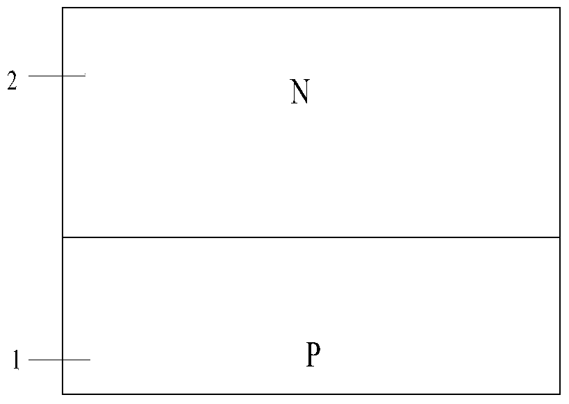
[0060] The first step: prepare a semiconductor material, the semiconductor material includes a substrate layer 1 and an active layer 2, the active layer 2 is located on the substrate layer 1, wherein the conductivity type of the substrate layer 1 is the second conductivity type, there are The conductivity type of the source layer 2 is the first conductivity type (such as figure 1 shown);

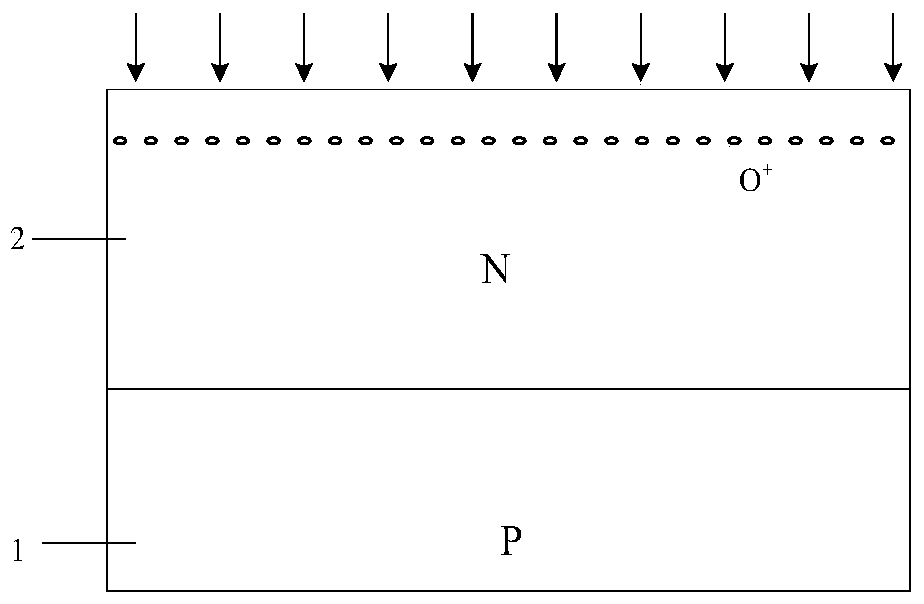
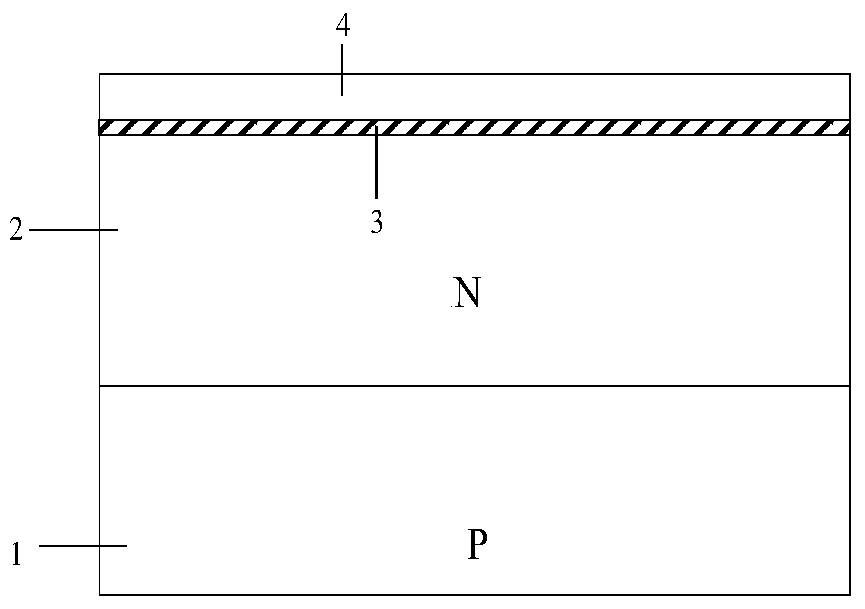
[0061] Step 2: Implant O on the surface of active layer 2 by ion implantation process + Ions (temperature 500-700 degrees, total dose 0.7e18cm -2 ~1.8e18cm -2 , implantation energy 70~200keV), form O in the active layer 2 + ionic layer (such as figure 2 shown); the annealing process is used to make the implanted ions react with the active layer material to form 80-200nm SiO 2 Isolation layer 3, SiO 2 An auxiliary semiconductor layer 4 (eg image 3 shown);

[0062] The third step: using ion impla...

Embodiment 2

[0069] The difference between this example and Example 1 is that the semiconductor material prepared in the first step also includes:

[0070] A dielectric buried layer 10, the dielectric buried layer 10 is located between the second conductivity type semiconductor substrate 1 and the first conductivity type semiconductor active layer 2 (such as Figure 10 shown). Figure 11 Shown is the complete LDMOS device fabricated.

Embodiment 3

[0072] The difference between this example and Example 1 lies in that the ions implanted on the upper layer of the semiconductor active layer 2 of the first conductivity type are N+.


PUM


Abstract

The invention belongs to semiconductor technology, and specifically relates to a manufacturing method of an LDMOS device. The main steps of the LDMOS device manufacturing method of the present invention are: forming a first conductive type semiconductor active layer on the upper surface of the second conductive type semiconductor substrate; implanting ions into the upper layer of the first conductive type semiconductor active layer to form a dielectric isolation layer, the The first conductive type semiconductor active layer on the upper surface of the dielectric isolation layer forms an auxiliary semiconductor layer; the second conductive type semiconductor impurities are implanted in the auxiliary semiconductor layer; the two ends of the auxiliary semiconductor layer are etched to the surface of the dielectric isolation layer to form a first active region A window and a second active region window; the body region and source metal are fabricated in the first active region window, and the drain contact region and drain metal are fabricated in the second active region window. The beneficial effect of the present invention is that the extended gate can be guaranteed to be made of single crystal silicon material, and the influence of the polycrystalline gate on the electrical performance of the extended gate device can be avoided.

Description

technical field [0001] The invention belongs to semiconductor technology, and in particular relates to a manufacturing method of an LDMOS (Lateral Double-diffusion Metal Oxide Semiconductor field effect transistor, lateral double-diffusion metal-oxide-semiconductor field effect transistor). Background technique [0002] Compared with VDMOS (Vertical Double-diffused MOSFET, vertical double-diffused metal-oxide-semiconductor field-effect transistor), LDMOS has the characteristics of fast switching speed and easy integration. Therefore, LDMOS is widely used in power integrated circuits, especially in radio frequency circuits. [0003] The key parameters of LDMOS are epitaxial layer thickness, doping concentration region and drift length. For conventional LDMOS, the specific on-resistance R on,sp There is a contradictory relationship between (specific on-resistance = on-resistance x device area) and withstand voltage BV: R on,sp ∝BV 2.5 . Reducing the doping concentration o...

Claims


Application Information

Patent Timeline
Patent Type & Authority Patents(China)
IPC IPC(8): H01L29/66H01L21/28
CPCH01L29/401H01L29/42356H01L29/42364H01L29/66681
Inventor 罗小蓉张彦辉刘建平谭桥尹超魏杰周坤马达徐青张波
Owner UNIV OF ELECTRONICS SCI & TECH OF CHINA
Why Eureka
Try Eureka