Semiconductor structure and forming method thereof

A technology of semiconductor and gate structure, applied in the field of semiconductor structure and its formation, can solve the problems that the performance and reliability of semiconductor devices need to be improved

Pending Publication Date: 2022-03-29
SEMICON MFG INT (SHANGHAI) CORP +1
View PDF0 Cites 0 Cited by
  • Summary
  • Abstract
  • Description
  • Claims
  • Application Information

AI Technical Summary

Problems solved by technology

[0004] However, the performance and reliability of semiconductor devices formed by existing technologies need to be improved

Method used


Image

  • Semiconductor structure and forming method thereof
  • Semiconductor structure and forming method thereof
  • Semiconductor structure and forming method thereof

Examples


Embodiment Construction

[0033] As mentioned in the background, the performance and reliability of existing fin field effect transistors still need to be improved. A detailed description will be given below in conjunction with the accompanying drawings.

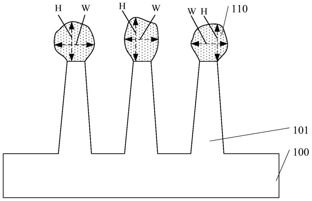
[0034] figure 1 It is a schematic cross-sectional structure diagram of a semiconductor structure.

[0035] Please refer to figure 1 , the semiconductor structure includes: a substrate 100; a fin 101 located on the substrate 100, the fin 101 has a source and drain opening (not shown); a source and drain doped layer 110 located in the source and drain opening, the The material of the source-drain doped layer 110 is silicon phosphide (SiP).

[0036] In the above embodiments, by making the material of the source-drain doped layer 110 contain phosphorus atoms, the stress formed by the source-drain doped layer 110 in the N-type MOS device can be increased to improve the performance of the semiconductor structure.

[0037] However, limited by the materi...


PUM

PropertyMeasurementUnit
widthaaaaaaaaaa
heightaaaaaaaaaa
thicknessaaaaaaaaaa

Abstract

The invention discloses a semiconductor structure and a forming method thereof, and the method comprises the steps: providing a substrate which comprises a substrate and a plurality of fin parts which are located on the substrate and are separated from one another, and the materials of the fin parts are provided with first atoms; forming an opening in the fin part; a source-drain doping layer is formed in the opening through the epitaxial growth technology, the source-drain doping layer comprises a seed layer located on the surface of the inner wall of the opening and a body layer located on the surface of the seed layer, first atoms, second atoms and third atoms are arranged in the material of the seed layer, and the first atoms and the second atoms are arranged in the material of the body layer. Therefore, the performance and the reliability of the fin field effect transistor are improved.

Description

technical field [0001] The invention relates to the field of semiconductor manufacturing, in particular to a semiconductor structure and a forming method thereof. Background technique [0002] With the rapid development of integrated circuit manufacturing technology, the size of semiconductor devices in the integrated circuit is continuously reduced, so that the operation speed of the entire integrated circuit will be effectively improved. [0003] In VLSI, stress is usually formed on the transistor to increase the carrier mobility of the transistor to increase the driving current of the transistor. [0004] However, the performance and reliability of semiconductor devices formed in the prior art need to be improved. Contents of the invention [0005] The technical problem solved by the invention is to provide a semiconductor structure and its forming method to improve the performance and reliability of the fin field effect transistor. [0006] In order to solve the abov...

Claims


Application Information

Patent Timeline
Patent Type & Authority Applications(China)
IPC IPC(8): H01L29/78H01L21/336
CPCH01L29/7848H01L29/785H01L29/66795H01L21/0262H01L21/02532H01L21/0245H01L21/02576H01L21/02639H01L29/165H01L29/0847H01L21/02645H01L29/7851
Inventor 刘震宇
Owner SEMICON MFG INT (SHANGHAI) CORP
Why Eureka
Try Eureka