Manufacturing method of interlayer film

A manufacturing method and interlayer film technology, applied in semiconductor/solid-state device manufacturing, electrical components, circuits, etc., can solve the problems of metal residues, affecting device performance, and adverse effects on the electrical performance of semiconductor devices, achieving no metal residues, avoiding The effect of electrical properties

Active Publication Date: 2020-10-09
SHANGHAI HUALI INTEGRATED CIRCUTE MFG CO LTD
View PDF2 Cites 0 Cited by
  • Summary
  • Abstract
  • Description
  • Claims
  • Application Information

AI Technical Summary

Problems solved by technology

[0019] However, by Figure 1D It can be seen that, due to the existence of the butterfly defect formed by the concave surface of the interlayer film 107, metal remains at the butterfly defect, and the residual metal is as marked 109a
[0020] Residual metal 109a obviously affects the performance of the device
In order to eliminate the influence of the residual metal 109a, the only way is to perform CMP to thin the interlayer film 107 and the metal gate 109, but the embedded silicon germanium layer 108 is prone to be exposed. risk, the exposure of the embedded silicon germanium layer 108 will adversely affect the electrical performance of the semiconductor device
At the same time, in order to eliminate the increased CMP of the residual metal 109a, the increase of the cost is also brought

Method used


Image

  • Manufacturing method of interlayer film
  • Manufacturing method of interlayer film
  • Manufacturing method of interlayer film

Examples


Embodiment Construction

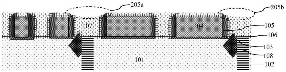
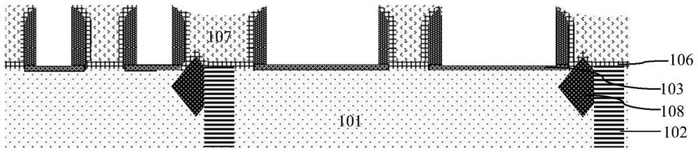
[0050] Such as figure 2 Shown is a flow chart of the manufacturing method of the interlayer film 7 in the embodiment of the present invention; Figure 3A to Figure 3C What is shown is a device structure diagram in each step of the method of the embodiment of the present invention. The method of manufacturing the interlayer film 7 of the embodiment of the present invention includes the following steps:

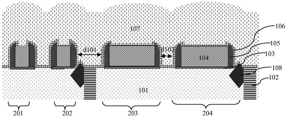
[0051] Step one, such as Figure 3A As shown, a semiconductor substrate 1 is provided on which a pattern structure of a semiconductor device is formed, and the area between each pattern structure is a pattern spacer.

[0052] In the embodiment of the present invention, the semiconductor substrate 1 is a silicon substrate.

[0053] The semiconductor device is a MOS transistor with HKMG. The interlayer film 7 is the zeroth interlayer film 7. Generally, the semiconductor device will be formed with multiple layers of metal, and the metal layers of each layer need to be isolated by inter...


PUM


Abstract

The invention discloses an interlayer film manufacturing method. The interlayer film manufacturing method comprises the following steps: step one, providing a semiconductor substrate on which a pattern structure of a semiconductor device is formed; step two, forming a first insulating layer on the bottom surface and side surfaces of the pattern spacer and the surface of the pattern structure outside the pattern spacer; step three, forming a second insulating layer to completely fill the pattern spacer and extend outside the pattern spacer; and step four: performing chemical mechanical polishing on the second insulating layer and the first insulating layer with the pattern structure as a stop layer, and forming the interlayer film formed by stacking the first and second insulating layers filled in the pattern spacer. The interlayer film manufacturing method can reduce or eliminate dishing defects on the interlayer film surface at the top of the pattern spacer, can improve the flatness of the entire interlayer film, and can improve the electrical properties of semiconductor devices.

Description

Technical field [0001] The invention relates to a method for manufacturing a semiconductor integrated circuit, in particular to a method for manufacturing an interlayer film. Background technique [0002] Such as Figure 1A to Figure 1E What is shown is a device structure diagram in each step of the existing manufacturing method of the interlayer film. The existing manufacturing method of the interlayer film 107 includes the following steps: [0003] Step one, such as Figure 1A As shown, a semiconductor substrate 101 is provided, and a pattern structure of a semiconductor device is formed on the semiconductor substrate 101, and the area between each pattern structure is a pattern spacer. [0004] Generally, the semiconductor substrate 101 is a silicon substrate. [0005] The semiconductor device is a MOS transistor with HKMG. HKMG has a high dielectric constant (HK) gate dielectric layer and a metal gate (MG), so it is usually abbreviated as HKMG in the art. [0006] The interlayer fi...

Claims


Application Information

Patent Timeline
Patent Type & Authority Patents(China)
IPC IPC(8): H01L21/31H01L21/3105H01L21/306
CPCH01L21/30625H01L21/31H01L21/31051
Inventor 李昱廷刘怡良却玉蓉龚昌鸿陈建勋
Owner SHANGHAI HUALI INTEGRATED CIRCUTE MFG CO LTD
Why Eureka
Try Eureka