

Detection Structure and Method for Mismatch Characteristics of Semiconductor Devices
A technology for detecting structure and detection method, which is applied in the direction of single semiconductor device testing, semiconductor devices, semiconductor/solid-state device components, etc., and can solve the problems of electrical parameter mismatch and the inability to fully and truly reflect product mismatch characteristics
- Summary
- Abstract
- Description
- Claims
- Application Information
AI Technical Summary
Problems solved by technology
Method used
Image

Examples
Embodiment Construction
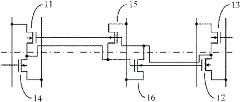
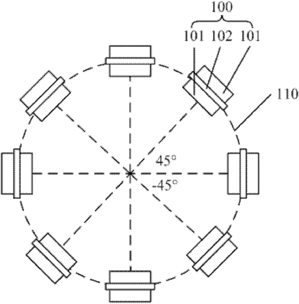
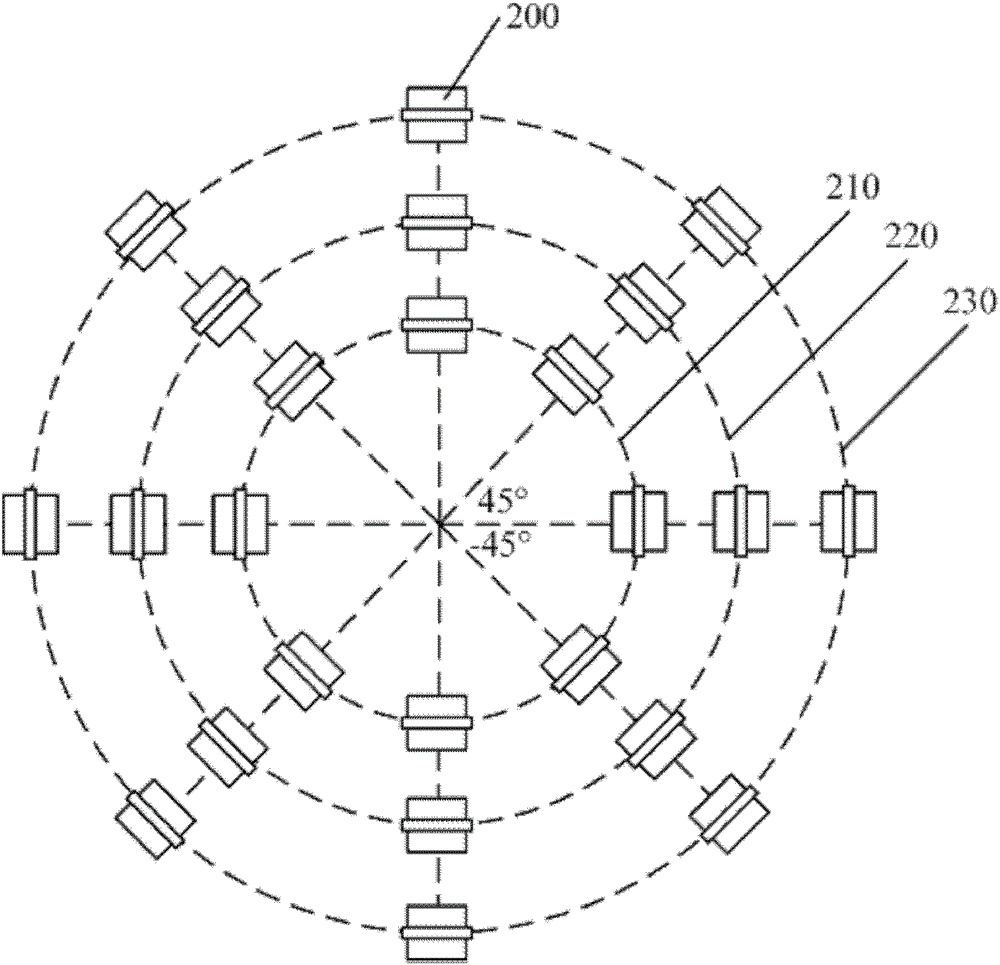
[0030] After an integrated circuit comprising two or more identical semiconductor devices is manufactured, the matching degree of the two or more identical semiconductor devices is often one of the main parameters for judging the performance of the integrated circuit. Since some integrated circuits are more sensitive to differences in electrical parameters of the same semiconductor device, that is, mismatch characteristics, it is necessary to understand the cause of the mismatch characteristics and minimize the mismatch characteristics. The method for obtaining the mismatch characteristics of semiconductor devices in the prior art is generally realized by computer simulation, and the method for obtaining the mismatch characteristics of the same semiconductor device using computer simulation is realized based on building a model, and the process of building a model It is an approximate description of the real situation, which cannot fully and truly reflect the mismatch character...
PUM
 Abstract
Description
Claims
Application Information