Connection structure of cable and printed circuit board (PCB)

A PCB board and connection structure technology, which is applied in the direction of connection, fixed connection, and parts of the connection device, can solve problems such as errors, mutual signal crosstalk, and impedance instability.

Inactive Publication Date: 2018-09-18
深圳市鼎电精密工业有限公司
View PDF10 Cites 5 Cited by
  • Summary
  • Abstract
  • Description
  • Claims
  • Application Information

AI Technical Summary

Problems solved by technology

[0002] See figure 1 As shown, the end of the connector is connected to the cable via the PCB board, and twin-core coaxial cables are commonly used in the cables. This kind of cable has a differential signal line pair inside (that is, the first differential signal line 1 and the second differential signal line Signal line 2), between adjacent differential signal line pairs and differential signal line pairs, it is easy to generate mutual signal crosstalk
[0003] The current PCB board 5 is provided with a GND PAD 4 (ground pad) between adjacent pairs of differential signal terminals, and the aforementioned cable is provided with a ground wire 3 (signal GND) in addition to the differential signal line pair. The ground wire 3 is welded to the corresponding GND PAD 4 to play an isolation role and reduce the mutual signal crosstalk between adjacent differential signal core wire pairs; usually, the shorter the better when the ground wire 3 is soldered, it is good for signal isolation Protection and characteristic impedance control, however, in the actual process, errors are prone to occur due to unstable changes during manual work, and the aforementioned grounding wires (usually bare copper wires) will be irregularly skewed, resulting in unstable characteristic impedance

Method used


Image

  • Connection structure of cable and printed circuit board (PCB)
  • Connection structure of cable and printed circuit board (PCB)
  • Connection structure of cable and printed circuit board (PCB)

Examples


Embodiment Construction

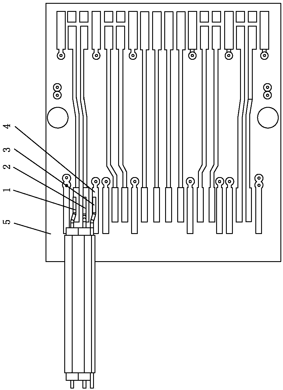
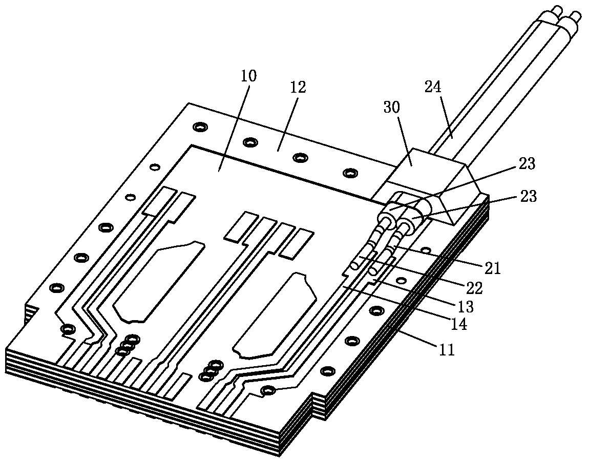
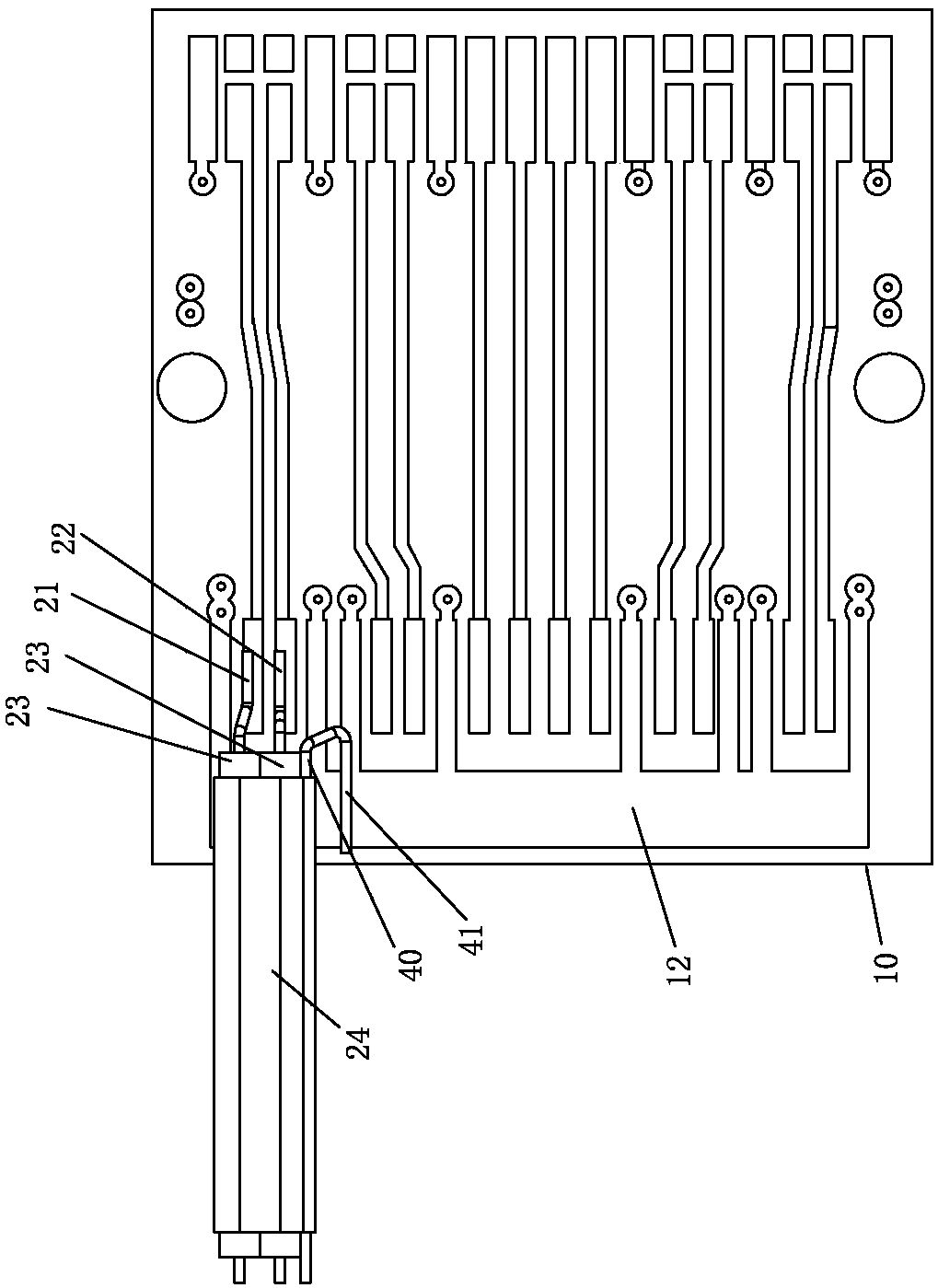
[0036] Please refer to Figure 2 to Figure 6 As shown, it shows the specific structure of two main embodiments of the present invention, which mainly solves the problem that the grounding wire in the prior art needs to be welded on the PCB board 10 in steps, and there are unstable changes during manual work. The grounding wire will be irregularly skewed, etc., which will cause problems such as uneven distance and unstable characteristic impedance.

[0037] Such as figure 2 As shown, it generally shows the specific structure of Embodiment 1 of the present invention, which includes a PCB board 10 and more than one cable (the expression "more than one cable" covers "one cable" , "two cables" and "multiple cables"), each cable has a differential signal line pair, an insulating layer 23 covering the outside of the differential signal line pair, and a metal shield covering the outside of the insulating layer 23 By 24 , the differential signal line pair includes a first differenti...


PUM


Abstract

The invention discloses a connection structure of a cable and a printed circuit board (PCB). The connection structure comprises the PCB and more than one cable, wherein each cable is provided with a differential signal line pair, an insulation layer and a metal shielding jacket, the insulation layer wraps the differential signal line pair, the metal shielding jacket wraps the insulation layer, a substrate is arranged on the PCB, a GND layer is arranged in the substrate, a signal end and a GND BAR are arranged on a surface of the substrate, the GND BAR is connected to the GND layer in a conduction layer, and the metal shielding jacket of the cable is pasted onto the GND BAR by conductive glue so as to achieve electrical conduction of the metal shielding jacket and the GND BAR; or a grounding metal wire is arranged in the cable, the grounding metal wire extends out of an end part of the metal shielding jacket and is returned back, and a return-back part of the grounding metal wire is electrically connected with the GND BAR for conduction. Therefore, the GND BAR is arranged on the PCB, the grounding metal wire is connected with the GND BAR or the metal shielding jacket is circuit-shorted with the GND BAR to achieve characteristic impedance matching, and an unstable variable during manual operation is effectively eliminated.

Description

technical field [0001] The invention relates to the technology in the field of circuit connection, in particular to a connection structure between a cable and a PCB board. Background technique [0002] See figure 1 As shown, the end of the connector is connected to the cable via the PCB board, and twin-core coaxial cables are commonly used in the cables. This kind of cable has a differential signal line pair inside (that is, the first differential signal line 1 and the second differential signal line Signal line 2), the problem of mutual signal crosstalk is likely to occur between adjacent differential signal line pairs and differential signal line pairs. [0003] The current PCB board 5 is provided with a GND PAD 4 (ground pad) between adjacent pairs of differential signal terminals, and the aforementioned cable is provided with a ground wire 3 (signal GND) in addition to the differential signal line pair. The ground wire 3 is welded to the corresponding GND PAD 4 to play...

Claims


Application Information

Patent Timeline
Patent Type & Authority Applications(China)
IPC IPC(8): H01R12/59H01R13/6581
CPCH01R12/59H01R13/6581
Inventor 张哲嘉
Owner 深圳市鼎电精密工业有限公司
Why Eureka
Try Eureka