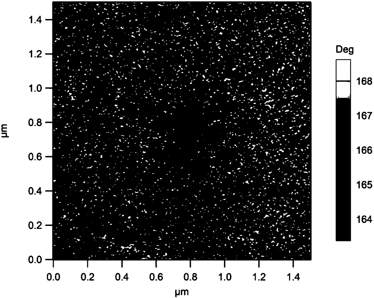
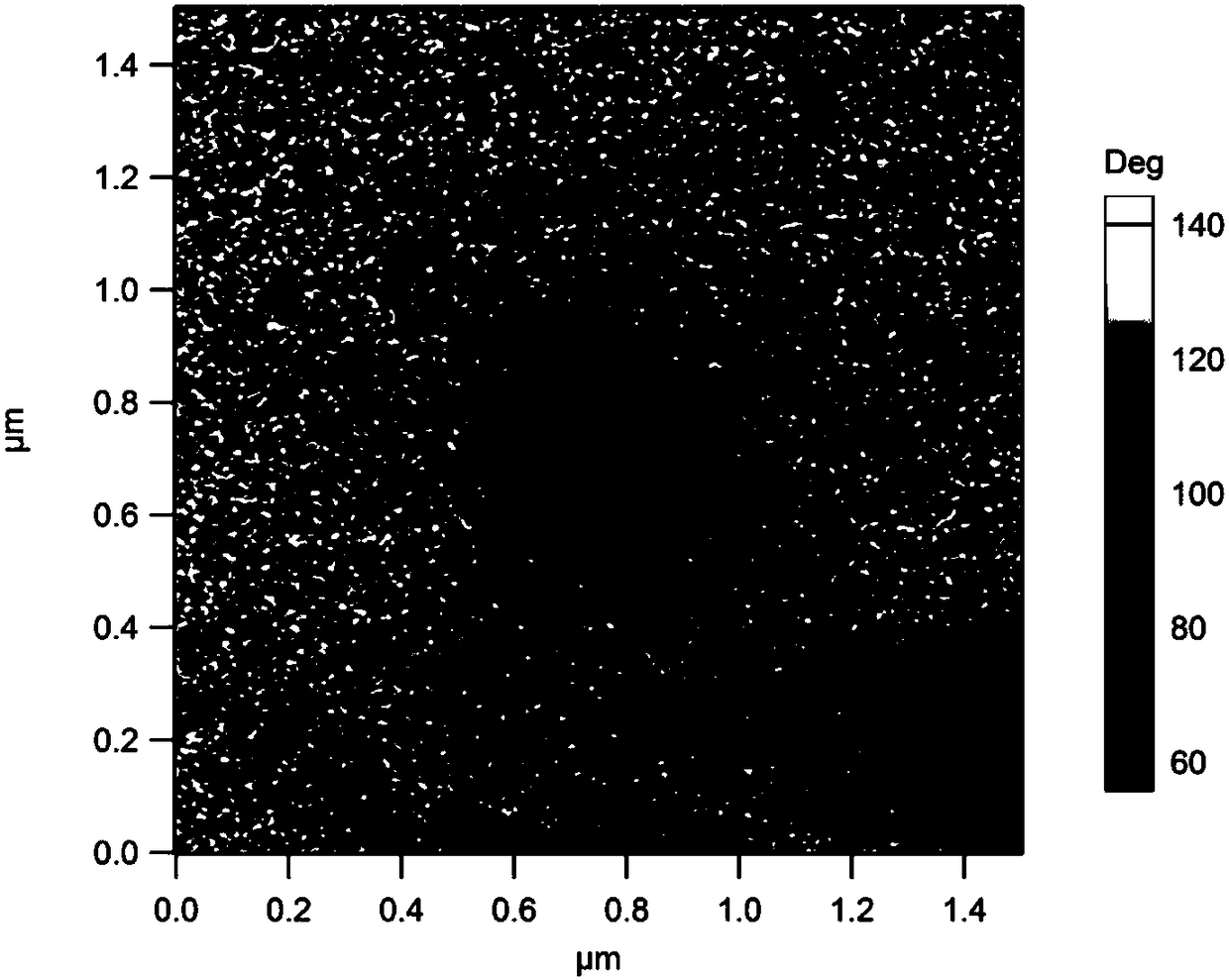
PFM-based lithium niobate nano-domain processing and imaging method
An imaging method, lithium niobate technology, applied in nanotechnology, chemical instruments and methods, crystal growth, etc., can solve problems such as difficult to obtain nanodomain structure
- Summary
- Abstract
- Description
- Claims
- Application Information
AI Technical Summary
Problems solved by technology
Method used
Image
Examples
Embodiment Construction
[0017] One, the present invention will be further described below in conjunction with embodiment.
[0018] A kind of lithium niobate nano-domain processing and imaging method based on PFM is carried out according to the following steps:
[0019] Step 1, scanning the surface of the lithium niobate thin film with a conductive probe applying a first AC voltage, the voltage value of the first AC voltage is less than the inversion voltage value of the iron domain of lithium niobate;
[0020] The lithium niobate film is a lithium niobate single crystal film polarized unidirectionally along the c-axis crystal axis;
[0021] In order to ensure the removal effect of the surface charge of the film, a conductive probe can be used for multiple scans;
[0022] Step 2, using a conductive probe that applies a first DC voltage to perform nano-domain processing on the scanned lithium niobate film, and the voltage value of the first DC voltage is greater than or equal to the reversal voltage v...
PUM
| Property | Measurement | Unit |
|---|---|---|
| Thickness | aaaaa | aaaaa |
| Thickness | aaaaa | aaaaa |
Abstract
Description
Claims
Application Information


