Display panel and preparation method thereof, and display device

A display panel and packaging layer technology, which is applied in the manufacture of semiconductor/solid-state devices, semiconductor devices, electrical components, etc., can solve the problems of short circuit, easy cracking or even breaking, affecting the display effect of the display panel, etc., and achieve the effect of ensuring integrity.

Active Publication Date: 2018-09-28
WUHAN TIANMA MICRO ELECTRONICS CO LTD
View PDF5 Cites 10 Cited by
  • Summary
  • Abstract
  • Description
  • Claims
  • Application Information

AI Technical Summary

Problems solved by technology

However, multiple small flexible display screens are spliced ​​together to form a foldable display panel, and then applied to large display devices. This splicing method is aimed at small display devices, such as mobile phones, tablet computers, etc. The effect is not ideal, which affects the display effect of the entire display panel
[0004] In addition, when the display panel is a flexible display panel, the bending reliability of the display panel is poor, and the repeated folding is easy to crack or even break, resulting in failure problems such as short circuit in the circuit, which affects the normal display of the display panel.

Method used

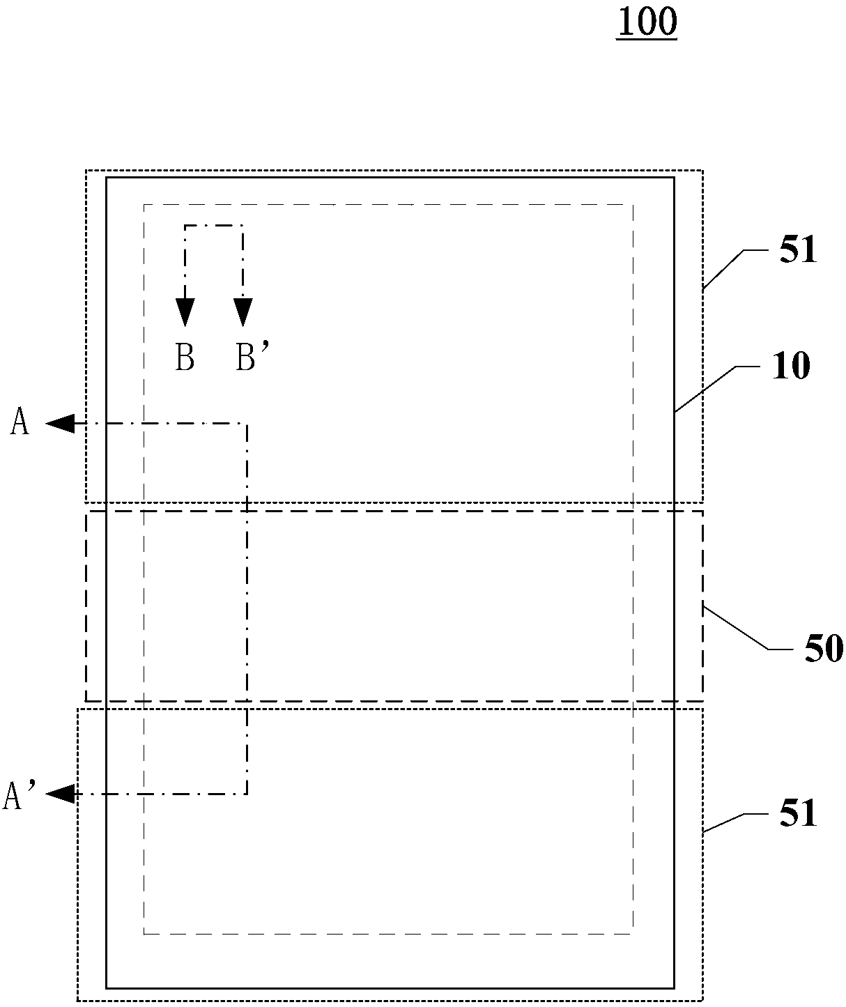
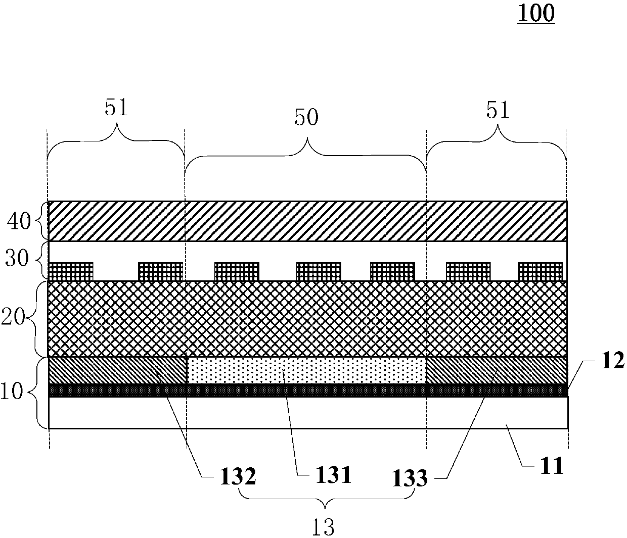
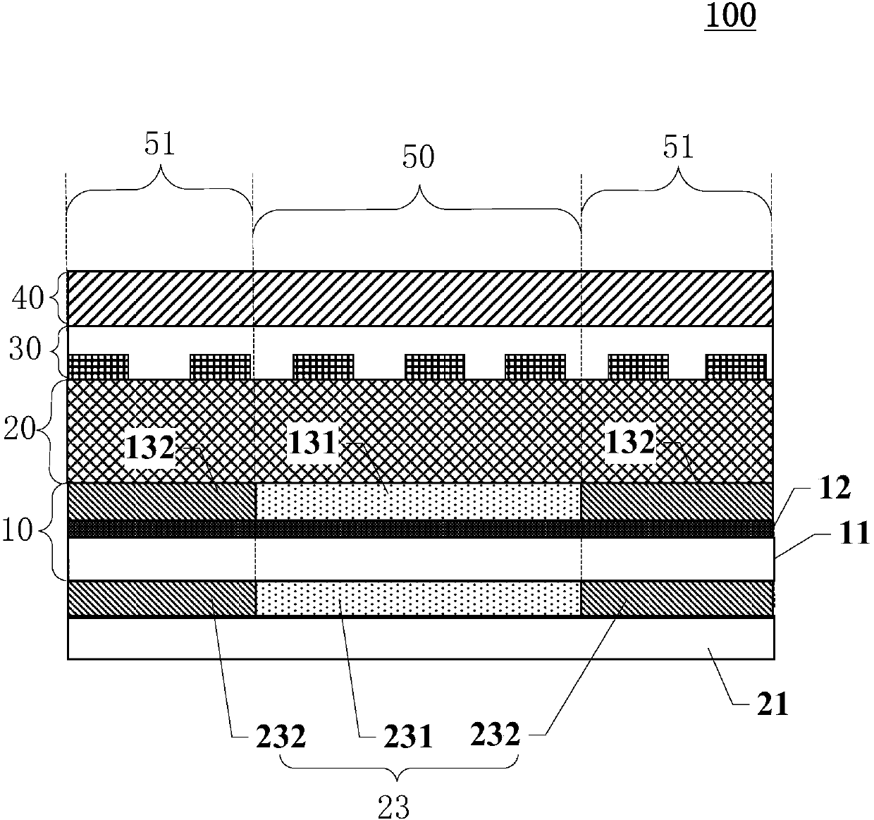

Image

  • Display panel and preparation method thereof, and display device
  • Display panel and preparation method thereof, and display device
  • Display panel and preparation method thereof, and display device

Examples


Embodiment Construction

[0033] Certain terms are used, for example, in the description and claims to refer to particular components. Those skilled in the art should understand that hardware manufacturers may use different terms to refer to the same component. The specification and claims do not use the difference in name as a way to distinguish components, but use the difference in function of components as a criterion for distinguishing. As mentioned throughout the specification and claims, "comprising" is an open term, so it should be interpreted as "including but not limited to". "Approximately" means that within an acceptable error range, those skilled in the art can solve the technical problem within a certain error range and basically achieve the technical effect. In addition, the term "coupled" herein includes any direct and indirect electrical coupling means. Therefore, if it is described that a first device is coupled to a second device, it means that the first device may be directly elect...


PUM


Abstract

The application discloses a display panel and a preparation method thereof, and a display device, and relates to the technical field of the display. A bending area and a non-bending area a provided, the display panel comprises at least one substrate, and a driving function layer, a light-emitting function layer and a package layer which are orderly arranged on the substrate along a direction far away from the substrate; the substrate comprises a first flexible base plate, and a first nano-film and a buffer layer orderly arranged on the first flexible base plate along a direction vertically faraway from the first flexible base plate, wherein the buffer layer is located at one side, close to the driving function layer, of the first nano-film, and comprises a first buffer layer located at the bending area and a second buffer layer located at the non-bending area, the first buffer layer and the second buffer layer are arranged at the same layer and have the same thickness, and the first buffer layer comprises organic materials. Therefore, the completeness of the first flexible base plate can be guaranteed, and the bending resistance of the display panel can be improved.

Description

technical field [0001] The present application relates to the field of display technology, in particular, to a display panel, a manufacturing method thereof, and a display device. Background technique [0002] In recent years, Organic Light-Emitting Diode (OLED) has become a very popular flat-panel display industry at home and abroad, and is hailed as the next-generation "star" flat-panel display technology, mainly because OLED has low power consumption. , Self-illumination, wide viewing angle, fast response time, high luminous efficiency, thin panel thickness, large-size and bendable panels can be produced, simple manufacturing process, and low cost. In addition, display devices with foldable performance are convenient to carry, and are an important development direction of display devices in the future. [0003] The existing foldable display panel can be opened and closed like a book, and has the advantages of small space occupation and convenient portability. At present...

Claims


Application Information

Patent Timeline
Patent Type & Authority Applications(China)
IPC IPC(8): H01L27/32H01L51/00H01L51/56
CPCH10K59/12H10K77/111H10K71/00Y02E10/549
Inventor 李莉达
Owner WUHAN TIANMA MICRO ELECTRONICS CO LTD
Why Eureka
Try Eureka