Display panel, manufacturing method thereof and display device

A technology for display panels and manufacturing methods, applied to semiconductor devices, electrical components, circuits, etc., can solve problems such as increased thickness of display panels, and achieve the effects of reducing complexity, area, and quantity

Inactive Publication Date: 2018-10-02
BOE TECH GRP CO LTD +1
View PDF5 Cites 4 Cited by
  • Summary
  • Abstract
  • Description
  • Claims
  • Application Information

AI Technical Summary

Problems solved by technology

[0004] The object of the present invention is to provide a display panel, its manufacturing method, and a display device, so as to solve

Method used


Image

  • Display panel, manufacturing method thereof and display device
  • Display panel, manufacturing method thereof and display device
  • Display panel, manufacturing method thereof and display device

Examples


Embodiment Construction

[0039] Embodiments of the present invention are described in detail below, examples of which are shown in the drawings, wherein the same or similar reference numerals designate the same or similar elements or elements having the same or similar functions throughout. The embodiments described below by referring to the figures are exemplary only for explaining the present invention and should not be construed as limiting the present invention.

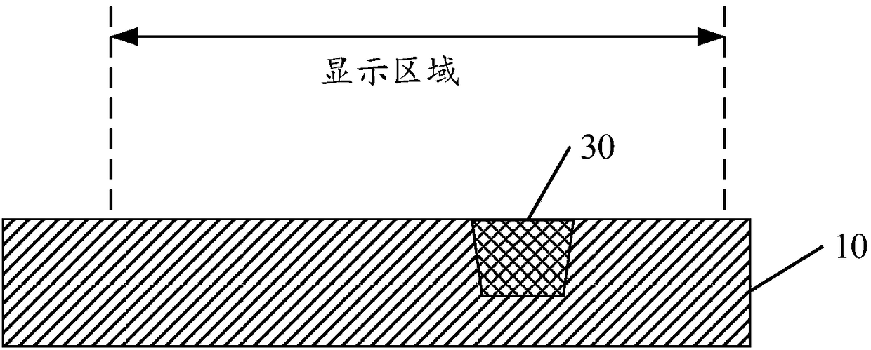
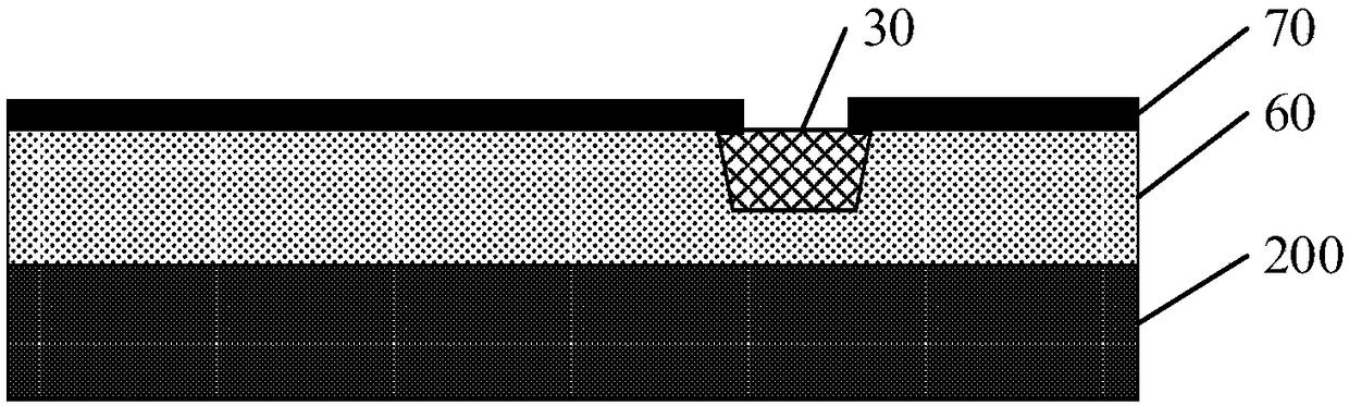
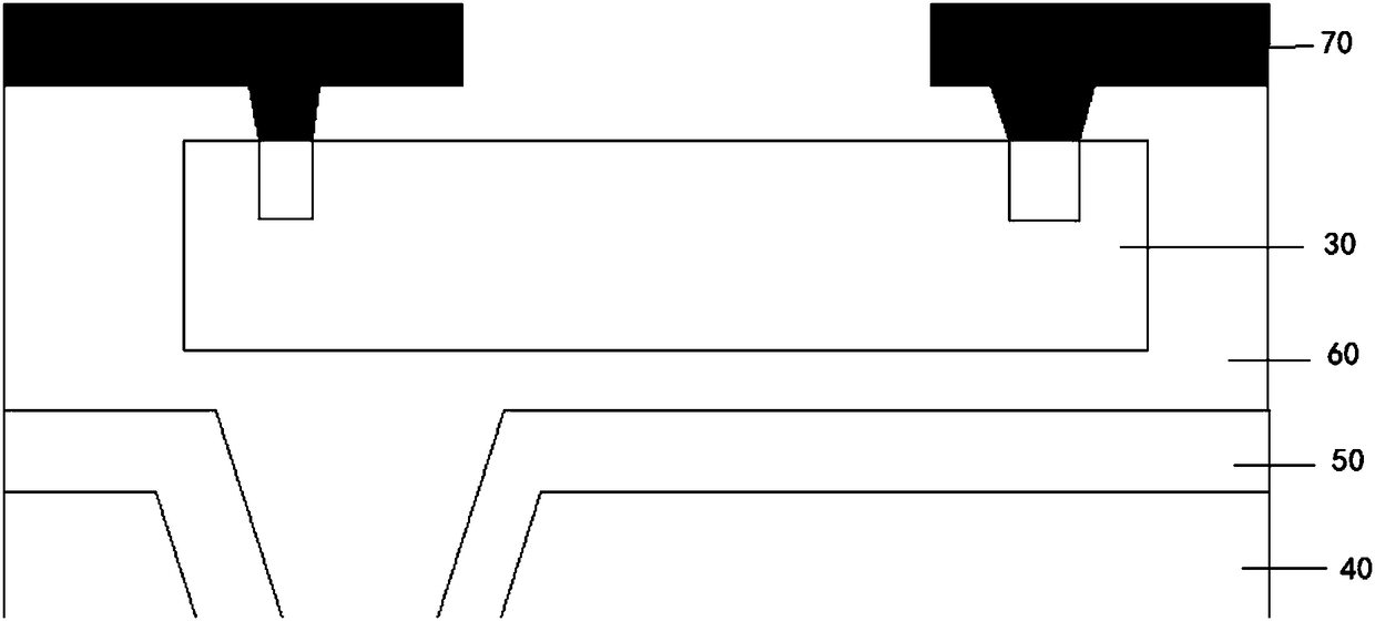
[0040] The present invention firstly provides a display panel, the structural diagram of which is as follows figure 1 As shown, it includes: a display structure 10 and a photoelectric sensing element 30 , the display area on the display structure 10 is provided with a groove, and the photoelectric sensing element 30 is embedded in the groove.

[0041] The display structure 10 includes a display area and a non-display area. The display structure may be a pixel driving circuit 80 and a planar layer 60 disposed thereon, or an array substra...


PUM


Abstract

The invention relates to the technical field of display, in particular to a display panel, a manufacturing method thereof and a display device. The display panel comprises a display structure and a photoelectric sensing element. A groove is arranged in the display region of the display structure. The photoelectric sensing element is embedded into the groove. According to the invention, the photoelectric sensing element is integrated in the display region of the display panel and the thickness of the display panel will not be increased.

Description

technical field [0001] The present invention relates to the field of display technology, in particular to a display panel, a manufacturing method thereof, and a display device. Background technique [0002] Ambient light sensors (Ambient light sensors, ALS) can sense the surrounding light conditions, and inform the processing chip to automatically adjust the brightness of the display backlight to reduce power consumption of the product. In the prior art, the photoelectric sensing device is located outside the display panel and is a separate system from the display panel, which is provided by the photoelectric device provider and the display panel provider respectively. The photoelectric sensing device module and the display panel are connected to each other through independent circuit paths. The control center is connected. This kind of plug-in connection method is difficult to align and the leads are complicated, which will cause assembly size and equipment tolerances, and ...

Claims


Application Information

Patent Timeline
IPC IPC(8): H01L27/12
CPCH01L27/1214H01L27/1259
Inventor 孙阔胡耀
Owner BOE TECH GRP CO LTD
Why Eureka
Try Eureka