Display panel and display panel manufacturing method

A technology for display panels and substrates, applied in semiconductor/solid-state device manufacturing, optics, instruments, etc., can solve problems such as increasing costs, and achieve the effects of cost control, low cost, and fewer masks

Pending Publication Date: 2022-03-15
WUHAN CHINA STAR OPTOELECTRONICS TECH CO LTD
View PDF0 Cites 1 Cited by
  • Summary
  • Abstract
  • Description
  • Claims
  • Application Information

AI Technical Summary

Problems solved by technology

During the research and practice of the existing technology, the inventors of the present application found that the current ambient light photosensitive elements basically adopt the plug-in method, which inevitably increases the production cost

Method used


Image

  • Display panel and display panel manufacturing method
  • Display panel and display panel manufacturing method
  • Display panel and display panel manufacturing method

Examples


Embodiment Construction

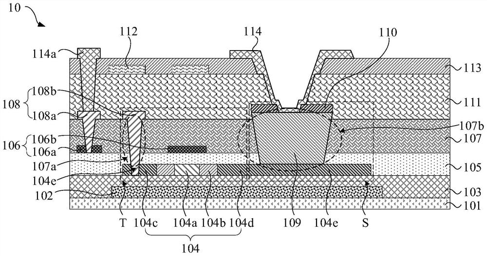
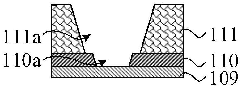
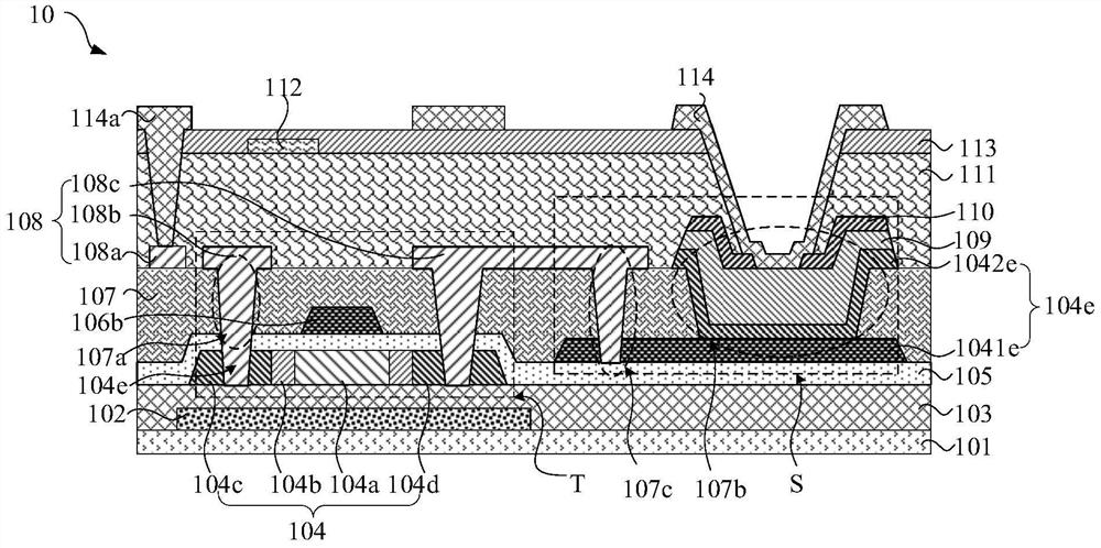
[0029] Next, the technical scheme in the present application embodiment will be described in the present application embodiment, and it is understood that the described embodiments are merely the embodiments of the present application, not all of the embodiments. Based on the embodiments in the present application, those skilled in the art will belong to the scope of this application without all other embodiments obtained without creative labor. Further, it should be understood that the specific embodiments described herein are for illustration and explanation of the present application is not intended to limit the present application. Nouns in the present application, in the absence of instructions to the contrary, as used "upper" and "lower" generally refers to the upper and lower means in actual use or operation state, in particular direction in the drawing plane of FIG. ; and "inner" and "outer" are terms for the profile of the device.

[0030] Embodiment of the present applic...


PUM


Abstract

The embodiment of the invention discloses a display panel and a display panel manufacturing method. The embodiment of the invention provides a photosensitive display panel with a novel integrated structure. According to the display panel provided by the embodiment of the invention, the photosensitive element is integrated on the array substrate. The photosensitive element and the thin film transistor device are arranged on the same side of the substrate. Some parts in the photosensitive element and some parts in the thin film transistor device can be manufactured in the same step, so that the integration level of the photosensitive element on the array substrate can be improved. In addition, after the integration level is improved, the influence on the thickness of the display panel can be reduced, and the display panel formed after integration is lighter and thinner. In addition, no extra process step is added, so that the manufacturing cost can be effectively controlled. Therefore, the photosensitive element can be integrated in the display panel with fewer photomasks and lower cost.

Description

Technical field [0001] The present application relates to the field of display technology, and particularly relates to a display panel, a display panel manufacturing method. Background technique [0002] With the rapid development of flat panel industry, people in addition to display high-resolution, wide viewing angle, low power consumption requirements, the display panel proposed other requirements. Wherein the ambient light detecting function can automatically adjust screen brightness according to the brightness of the external environment, in accordance with the external environment can be automatically open when the flash photographing or fill light. In the research and practice of the prior art, the present inventors have found application, ambient light sensor now have adopted the basic plug mode, so inevitably increases the cost of production. Inventive content [0003] Example embodiments of the present application provides a display panel and a display panel manufactur...

Claims


Application Information

Patent Timeline
Patent Type & Authority Applications(China)
IPC IPC(8): H01L27/12H01L21/77G02F1/1368G02F1/1362G02F1/167G02F1/1676G02F1/1677
CPCH01L27/1214H01L27/124H01L27/1259G02F1/1368G02F1/136286G02F1/167G02F1/1676G02F1/1677
Inventor 宋继越艾飞宋德伟龚帆
Owner WUHAN CHINA STAR OPTOELECTRONICS TECH CO LTD
Why Eureka
Try Eureka