
Constant voltage output circuit

A constant voltage, output circuit technology, applied to electrical components, adjusting electrical variables, power oscillators, etc., can solve problems such as changes in bias current values, and achieve the effects of reducing output voltage deviation and low power consumption

Active Publication Date: 2021-09-24
SII SEMICONDUCTOR CORP
View PDF6 Cites 0 Cited by
  • Summary
  • Abstract
  • Description
  • Claims
  • Application Information

AI Technical Summary

Problems solved by technology

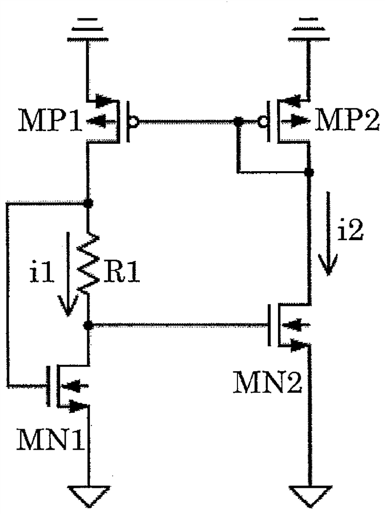
However, in Figure 4 In the bias current control circuit as shown, there is a problem that the bias current value fluctuates according to the variation of the resistance element in the bias current control circuit.

Method used


Image

  • Constant voltage output circuit
  • Constant voltage output circuit
  • Constant voltage output circuit

Examples


no. 1 approach )

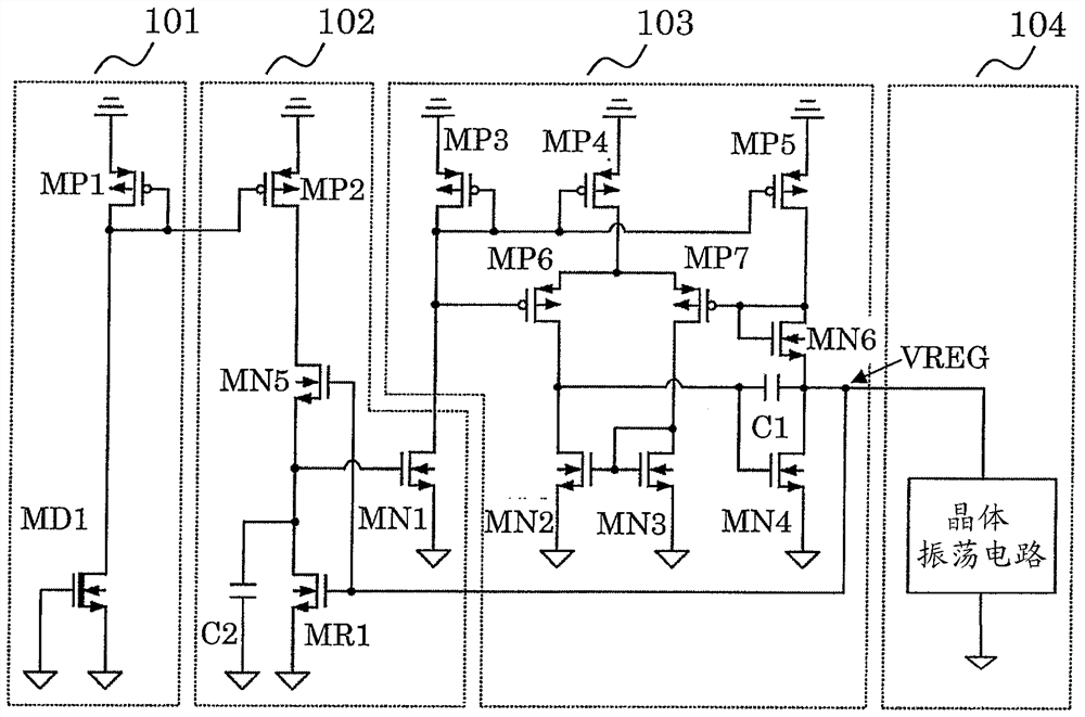
[0019] exist figure 1 The first embodiment of the constant voltage output circuit of the present invention is shown in . The constant voltage output circuit of this embodiment is as figure 1 As shown, a constant current circuit 101, a bias current control circuit 102, and a constant voltage circuit 103 are provided. The constant current circuit 101 is composed of an N-channel depletion transistor (depletion transistor) MD1 and a PMOS transistor MP1. Bias current control circuit 102 is composed of PMOS transistor MP2 and NMOS transistors MN1, MN5, and MR1. The constant voltage circuit 103 is composed of PMOS transistors MP3, MP4, MP5, MP6, MP7 and NMOS transistors MN2, MN3, MN4, MN6. Let the output node of the constant voltage circuit 103 be the VREG node, and let the voltage between the power supply and the VREG node be the voltage of the VREG node.

[0020] The connection of the constant current circuit 101 will be described. Connect the source terminal of transistor M...

no. 2 approach )

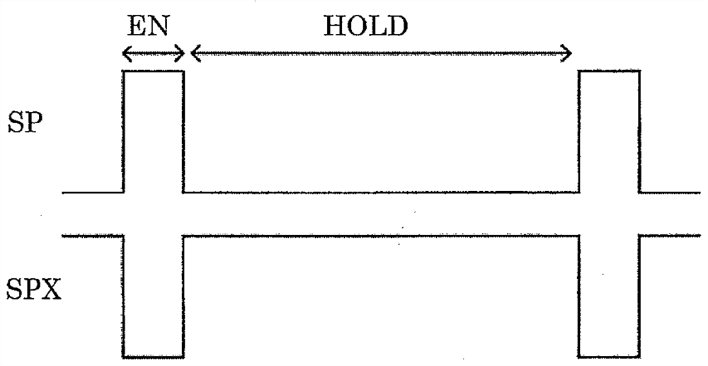
[0029] exist figure 2 A second embodiment of the constant voltage output circuit of the present invention is shown in . This circuit structure is used to reduce the power consumption of the constant voltage output circuit itself. In this embodiment, a switch for performing a sample-and-hold operation, a sample-and-hold signal generating circuit for generating a signal for causing the switch to perform the sample-and-hold operation, and a hold circuit are provided. generate image 3 The shown sample-and-hold signal is applied to the switch, and the operation of the constant voltage circuit is stopped to maintain the state when it is enabled, thereby reducing power consumption.

[0030] Differences in configuration between the second embodiment and the first embodiment will be described. Such as figure 2 As shown, the constant current circuit 101 and the bias current control circuit 102 are the same as those of the first embodiment.

[0031] Differences in the configurati...


PUM


Abstract

The invention relates to a constant voltage output circuit. The output voltage deviation is reduced to obtain a constant voltage output circuit with low power consumption. By providing the bias current control circuit controlled by the constant voltage output of the constant voltage output circuit, the constant voltage output deviation caused by the current deviation of the constant current source is reduced.

Description

technical field [0001] The invention relates to a constant voltage output circuit. Background technique [0002] In a low-power crystal oscillator circuit used in an electronic clock or the like, the crystal oscillator circuit is generally operated based on the output voltage of a constant voltage output circuit in order to reduce current consumption. The setting of this output voltage is set so that the difference between the operation start voltage of the crystal oscillation circuit and the output voltage of the constant voltage circuit is fixed as in Patent Document 1, thereby realizing stable crystal oscillation without causing an increase in power consumption. Work. At this time, the output voltage of the constant voltage output circuit is determined by the sum of the voltages of the diode junction lines of the P-channel MOS (hereinafter abbreviated as PMOS) transistor and the N-channel MOS (hereinafter abbreviated as NMOS) transistor. [0003] prior art literature ...

Claims


Application Information

Patent Timeline
Patent Type & Authority Patents(China)
IPC IPC(8): G05F1/56
CPCG05F1/56H03B5/04H03B2200/006G05F1/565H03B5/32G05F1/59G05F1/575
Inventor 佐野稔
Owner SII SEMICONDUCTOR CORP
Learn More