
Rapid positioning and batch detection method for micro-defects on the surface of large-aperture optical crystals

An optical crystal, batch detection technology, applied in the field of optical engineering, can solve problems affecting the quality and efficiency of micro-defect repair, and achieve the effect of saving image acquisition efficiency and accurate positioning

Active Publication Date: 2021-09-07
HARBIN INST OF TECH
View PDF11 Cites 0 Cited by
  • Summary
  • Abstract
  • Description
  • Claims
  • Application Information

AI Technical Summary

Problems solved by technology

Therefore, it is urgent to develop an efficient and stable batch automatic detection system that cannot rely solely on manual operations; in addition, the reliable identification of micro-defect points on the surface of large-diameter KDP crystals and the precise search for defect locations directly affect the quality and efficiency of micro-defect repair

Method used


Image

  • Rapid positioning and batch detection method for micro-defects on the surface of large-aperture optical crystals
  • Rapid positioning and batch detection method for micro-defects on the surface of large-aperture optical crystals
  • Rapid positioning and batch detection method for micro-defects on the surface of large-aperture optical crystals

Examples


specific Embodiment approach 1

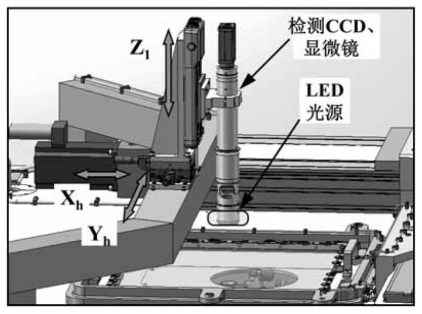
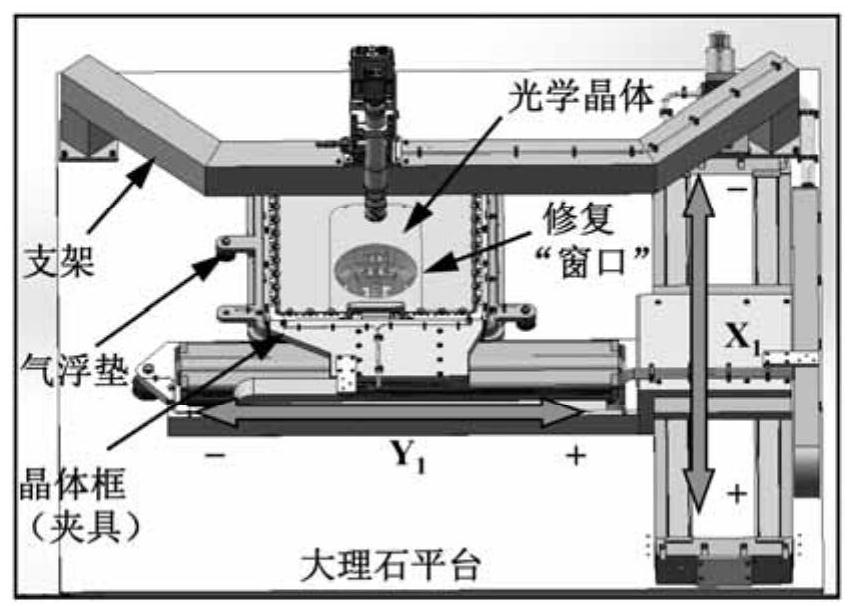
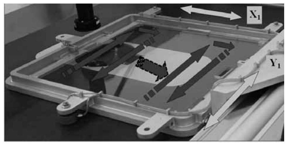
[0050] Specific implementation mode one: as Figures 1 to 7 As shown, the rapid location and batch detection method for micro-defects on the surface of large-aperture optical crystals described in this embodiment is implemented by the following steps:

[0051] 1. Install the optical crystal element to be tested, assemble and adjust the micro-defect detection microscope system, and automatically return to zero on each axis of the crystal element moving mechanism;

[0052] 2. Determine the actual magnification of the microscope based on the raster scanning path of large-diameter components, estimate the field of view of the CCD for defect detection under different magnifications, and select the scanning step for micro-defects on the surface of the entire crystal component;

[0053] 3. Compare the two scanning schemes of "continuous motion acquisition" and "intermittent stop acquisition" in terms of defect scanning efficiency and imaging quality, and formulate a reasonable scanni...


PUM


Abstract

The invention relates to a rapid location-finding and batch detection method for micro-defects on the surface of large-diameter optical crystals, which belongs to the field of optical engineering. The invention is proposed to solve the problem of batch, fast and accurate detection of micro-defects on the surface of large-diameter optical crystals. The method first adopts the "continuous motion acquisition" raster scanning method to completely scan the entire crystal element; then, by developing an image acquisition program and establishing its communication with the numerical control motion program, the function of acquiring images according to the real-time scanning position of the crystal is realized; Based on the image processing algorithm, the ellipse fitting of the contour position of the defect point in the collected image is realized, and information such as the number, position, and size of the defect point in a single image is obtained; finally, the automatic detection program of the defect point is developed, and the micro-defect information based on Microsoft Access is established. Database to realize batch detection of collected images and storage and update of defect point information. The invention also provides detailed parameter basis for the repair and control of micro-defects on the surface of the large-diameter crystal element.

Description

technical field [0001] The invention belongs to the field of optical engineering, and in particular relates to a rapid location-finding and batch detection method for micro-defects on the surface of large-diameter optical crystals. Background technique [0002] With the rapid development of human society, the shortage of fossil fuels on the earth is becoming more and more serious. Nuclear fusion energy has become the goal that countries all over the world have been pursuing in recent years because of its advantages of abundance, cleanliness and high efficiency. Establishing a large-scale high-energy solid-state laser device is the key to realizing controlled nuclear fusion, and the output energy of the laser nuclear fusion device also directly determines whether the nuclear fusion ignition is successful or not. In order to achieve high-energy output, laser nuclear fusion devices need to use large-scale, high-precision, and high-quality optical components in large quantities...

Claims


Application Information

Patent Timeline
Patent Type & Authority Patents(China)
IPC IPC(8): G01N21/88
CPCG01N21/8851G01N2021/8887
Inventor 程健陈明君左泽轩刘启杨浩赵林杰王廷章刘志超王健许乔
Owner HARBIN INST OF TECH
Learn More