Zero temperature drift current bias circuit

A current bias, zero temperature drift technology, applied in the direction of adjusting electrical variables, control/regulating systems, instruments, etc., can solve the problems of different process fluctuations, and achieve the effect of easy implementation, ingenious overall structure design, simple and reasonable structure

Active Publication Date: 2018-10-12
SUZHOU KAIWEITE SEMICON
View PDF8 Cites 10 Cited by
  • Summary
  • Abstract
  • Description
  • Claims
  • Application Information

AI Technical Summary

Problems solved by technology

However, there is a serious problem in this circuit, because RA and RB are resistors of different materials, so they are affected differently by process fluctuations

Method used


Image

  • Zero temperature drift current bias circuit
  • Zero temperature drift current bias circuit
  • Zero temperature drift current bias circuit

Examples


Embodiment Construction

[0019] In order to deepen the understanding and recognition of the present invention, the present invention will be further described and introduced below in conjunction with the accompanying drawings.

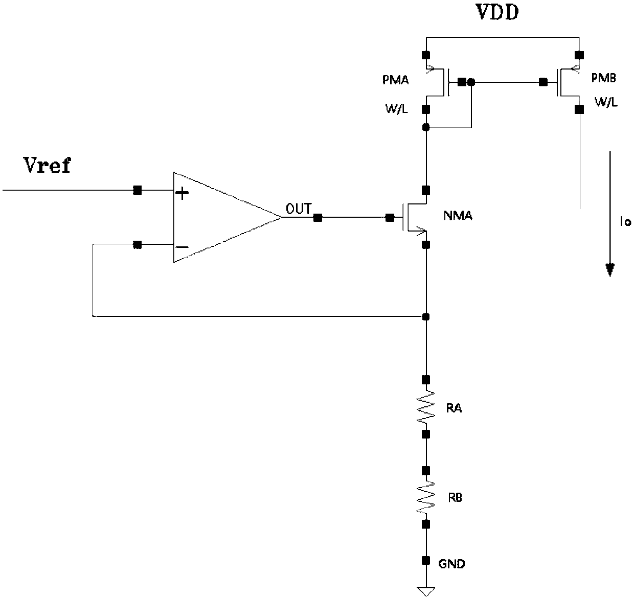
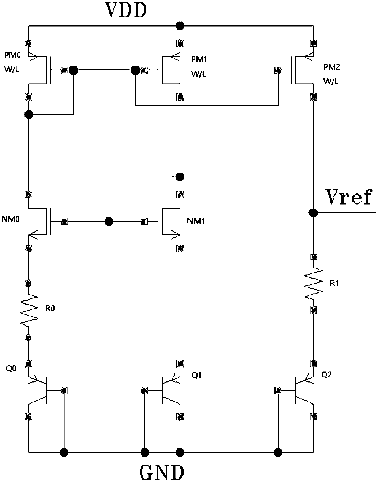
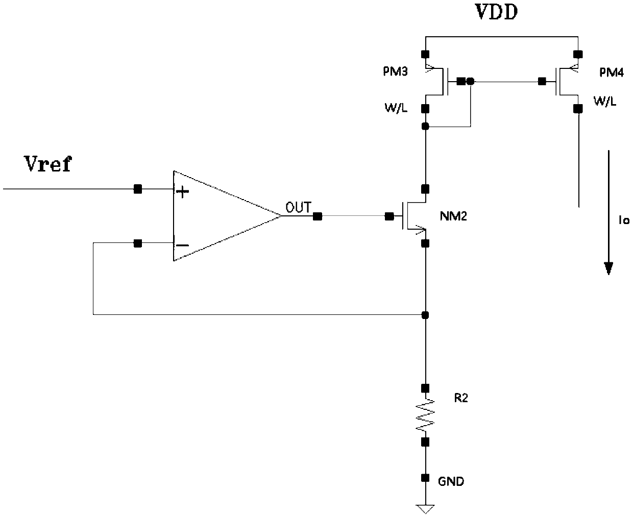
[0020] Such as Figure 2-3 As shown, a zero temperature drift current bias circuit includes a reference voltage generation circuit and a bias current generation circuit, the reference voltage generation circuit includes a first MOS transistor PM0, a second MOS transistor PM1, a third MOS transistor PM2, The fourth MOS transistor NM0, the fifth MOS transistor NM1, the first transistor Q0, the second transistor Q1, the third transistor Q2, the first resistor R0 and the second resistor R1, the first MOS transistor PM0 , The second MOS transistor PM1 and the third MOS transistor PM2 adopt a cascode structure, and the source is connected to the power supply VDD, the drain of the first MOS transistor PM0 is connected to the drain of the fourth MOS transistor NM0, and the first MOS t...


PUM


Abstract

The invention relates to a zero temperature drift current bias circuit. The circuit comprises a reference voltage generating circuit and a bias current generating circuit, wherein the reference voltage generating circuit comprises a first MOS transistor, a second MOS transistor, a third MOS transistor, a fourth MOS transistor, a fifth MOS transistor, a first triode, a second triode, a third triode, a first resistor and a second resistor. The first MOS transistor, the second MOS transistor and the third MOS transistor adopt a cascode structure. The first resistor is connected between a source of the fourth MOS transistor and an emitter of the first triode, a source of the fifth MOS transistor is connected to an emitter of the second triode, and the second resistor is connected between a drain of the third MOS transistor and an emitter of the third triode. Bases and collectors of the first triode, the second triode and the third triode are grounded. The bias current generating circuit includes an operational amplifier, a sixth MOS transistor, a seventh MOS transistor, an eighth MOS transistor and a third resistor. The reference voltage generating circuit is connected to the positiveinput end of the operational amplifier, and the third resistor is connected between a source of the sixth MOS transistor and the ground.

Description

technical field [0001] The invention relates to the field of integrated circuit design, in particular to a current bias circuit, in particular to a current bias circuit with zero temperature drift. Background technique [0002] In the field of integrated circuit design, integrated circuits with various functions are almost inseparable from current bias circuits. In some applications, we need to use a current bias circuit with zero temperature drift, that is, the magnitude of the current bias does not change with temperature. [0003] The usual zero temperature drift current circuit generation method is as follows figure 1 As shown, Vref is a reference voltage that is not affected by temperature, RA and RB are resistors of different materials, RA is a resistor with positive temperature characteristics (that is, the resistance of RA will become larger when the temperature rises), and RB is a negative temperature characteristic The resistance (that is, the resistance value of...

Claims


Application Information

Patent Timeline
Patent Type & Authority Applications(China)
IPC IPC(8): G05F1/567
CPCG05F1/567
Inventor 张胜谭在超丁国华罗寅
Owner SUZHOU KAIWEITE SEMICON
Why Eureka
Try Eureka