
Electromagnetic folding clamp for polycrystalline silicon wafer

A polycrystalline silicon wafer, electromagnetic technology, applied in the direction of conveyor objects, transportation and packaging, can solve problems such as complex structure, achieve the effect of simple fixture structure, save maintenance costs, and avoid damage

Inactive Publication Date: 2018-10-16
SUZHOU SUNWELL NEW ENERGY CO LTD
View PDF10 Cites 1 Cited by
  • Summary
  • Abstract
  • Description
  • Claims
  • Application Information

AI Technical Summary

Problems solved by technology

[0003] For the current method of producing solar polysilicon wafers, it is often necessary to transfer the polysilicon wafers for further processing during production, but now the jig for transferring polysilicon wafers is clamped after being sucked by a suction cup, and the structure is complicated.

Method used


Image

  • Electromagnetic folding clamp for polycrystalline silicon wafer

Examples


Embodiment 1

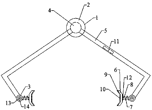
[0019] An electromagnetic folding fixture for polycrystalline silicon wafers, comprising: a folding support 1, the folding support 1 is composed of a folding device 2 and two rotating arms 5, and one end of the two rotating arms 5 is connected to the folding device 2 .

[0020] The folding motor 4 is installed on the rotating arm 5, and the folding motor 4 is embedded in the folding device 2. The folding motor 4 is used to adjust the angle of the two rotating arms 5, so as to achieve the purpose of clamping .

[0021] The bottom end of the rotating arm 5 is equipped with a fixed clip 6, the fixed clip 6 is installed on the rotating arm 5 through a slide bar 7, and the fixed clip 6 is sleeved on the slide bar 7 through a round hole. The fixing clip 6 is slidably connected to the sliding bar 7, so that the fixing clip 6 can slide on the sliding bar 7, thereby adapting to products of different sizes.

[0022] The slide bar 7 is covered with a spring 8, and the two ends of the s...

Embodiment 2

[0031] An electromagnetic folding fixture for polycrystalline silicon wafers, comprising: a folding support 1, the folding support 1 is composed of a folding device 2 and two rotating arms 5, and one end of the two rotating arms 5 is connected to the folding device 2 .

[0032] The folding motor 4 is installed on the rotating arm 5, and the folding motor 4 is embedded in the folding device 2. The folding motor 4 is used to adjust the angle of the two rotating arms 5, so as to achieve the purpose of clamping .

[0033] The bottom end of the rotating arm 5 is equipped with a fixed clip 6, the fixed clip 6 is installed on the rotating arm 5 through a slide bar 7, and the fixed clip 6 is sleeved on the slide bar 7 through a round hole. The fixing clip 6 is slidably connected to the sliding bar 7, so that the fixing clip 6 can slide on the sliding bar 7, thereby adapting to products of different sizes.

[0034] The slide bar 7 is covered with a spring 8, and the two ends of the s...


PUM


Abstract

The invention discloses an electromagnetic folding clamp for a polycrystalline silicon wafer. The electromagnetic folding clamp comprises a folding support, and the folding support is composed of a folding device and two rotary arms. Fixed clamps are mounted at the bottom ends of the rotary arms, and adjusting devices are mounted between the rotary arms and the fixed clamps. A gyroscope and an adjusting motor are mounted in each adjusting device, and electromagnets are mounted in the fixed clamps. Buffer mats are mounted on the opposite faces of the two fixed clamps, and pressure inductors aremounted between the buffer mats and the fixed clamps. A processing chip is mounted on the folding support, and connected with the gyroscopes, the adjusting motors, a folding motor, the electromagnetsand the pressure inductors through wires. In this manner, the electromagnetic folding clamp for the polycrystalline silicon wafer is simple in structure, the polycrystalline silicon wafer can be directly clamped, the polycrystalline silicon wafer can be prevented from being damaged, and maintenance costs are saved.

Description

technical field [0001] The invention relates to the field of solar energy equipment, in particular to an electromagnetic folding fixture for polycrystalline silicon wafers. Background technique [0002] Now with the development of science and technology, solar polysilicon wafers are often used in some devices. Since polysilicon wafers can integrate tens of millions of transistors in a very small area, the engineering is extremely high, especially in the current microelectronics In the field of technology, aerospace, industry, agriculture and commerce are also widely used. [0003] For the current method of producing solar polysilicon wafers, it is often necessary to transfer the polysilicon wafers during production for further processing, but now the clamps for transferring polysilicon wafers are clamped after being absorbed by suction cups, and the structure is complicated. Contents of the invention [0004] The technical problem mainly solved by the present invention is...

Claims


Application Information

Patent Timeline
IPC IPC(8): B65G47/90
CPCB65G47/90
Inventor 李中天
Owner SUZHOU SUNWELL NEW ENERGY CO LTD
Learn More