Electric connecting structure, display panel and connecting-binding method of conductive connecting part thereof
An electrical connection structure and display panel technology, applied in nonlinear optics, instruments, optics, etc., can solve the problems of bonding process failure, inability to crush, conductive particle aggregation, etc., to improve the failure risk and improve the yield effect.
- Summary
- Abstract
- Description
- Claims
- Application Information
AI Technical Summary
Problems solved by technology
Method used
Image

Examples
Embodiment 1
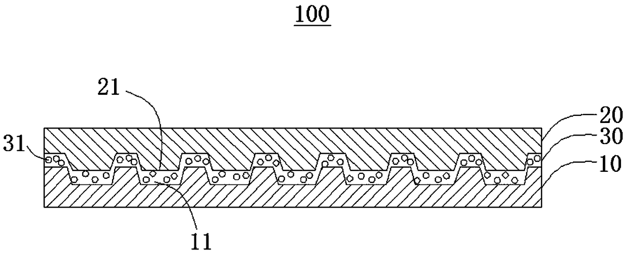
[0033] figure 1 is a side cross-sectional view of the electrical connection structure according to Embodiment 1 of the present invention.
[0034] refer to figure 1 , according to Embodiment 1 of the present invention, an electrical connection structure is proposed. The electrical connection structure includes a first conductive adhesive layer 10 , an anisotropic conductive adhesive layer 30 and a second conductive adhesive layer 20 which are sequentially stacked. Of course, the present invention is not limited thereto, and the electrical connection structure may also include other necessary components.
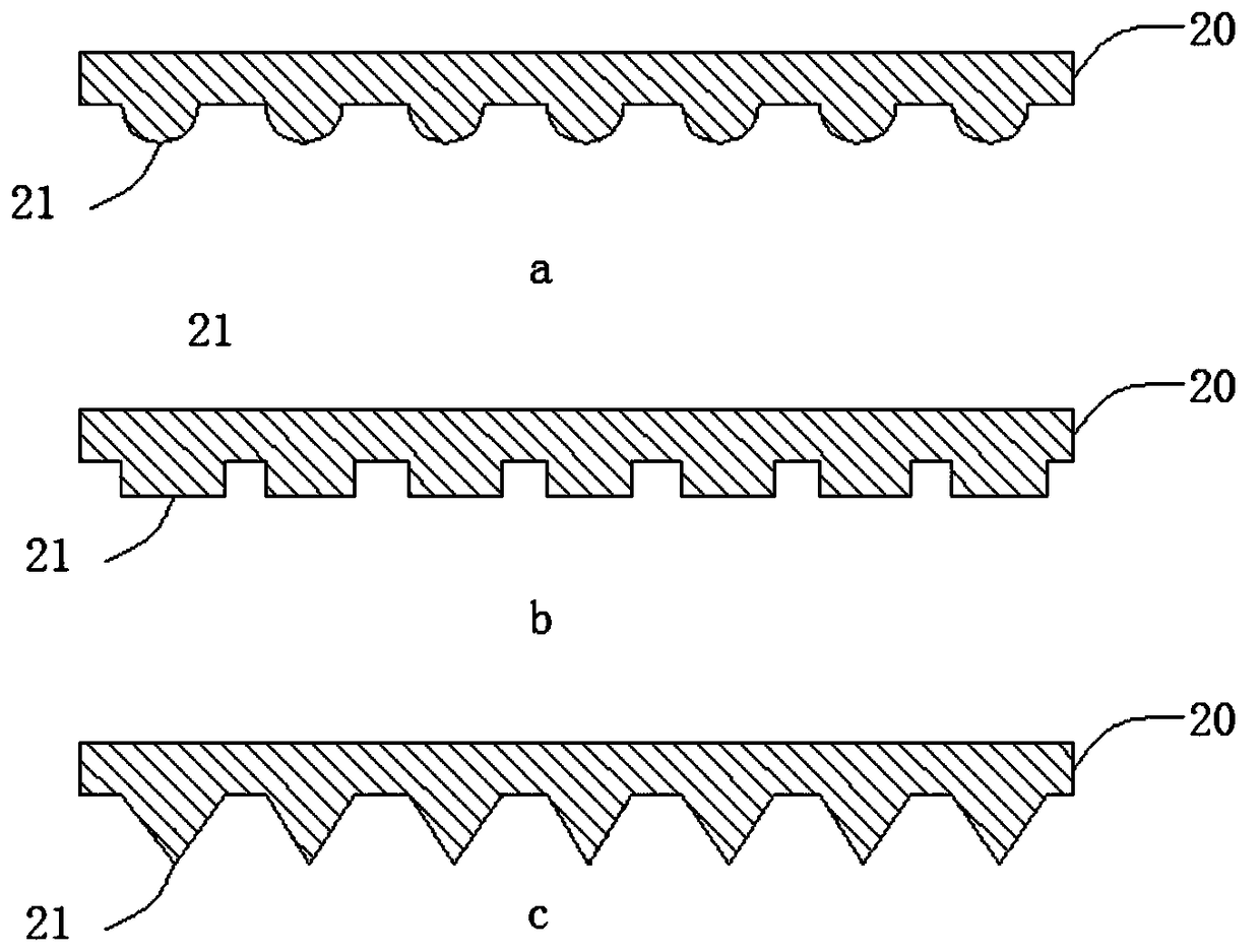
[0035] Specifically, the surface of the first conductive adhesive layer 10 facing the anisotropic conductive adhesive layer 30 has a plurality of grooves 11 . The surface of the second conductive adhesive layer 20 facing the anisotropic conductive adhesive layer has a plurality of protrusions 21 matching the grooves 11 . The protrusion 21 is accommodated in the groove 11 ...
Embodiment 2
[0044] image 3 is a top view of the display panel according to Embodiment 2 of the present invention. Figure 4 It is a side cross-sectional view of the electrical connection structure of the display panel according to Embodiment 2 of the present invention before hot pressing. Figure 5 It is a side cross-sectional view of the electrical connection structure of the display panel according to the second embodiment of the present invention after hot pressing.
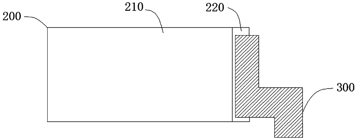
[0045] refer to image 3 , Figure 4 and Figure 5As shown, a display panel is provided according to Embodiment 2 of the present invention. The display panel includes a display part 200 and a binding part 300 located at a side of the display part 200 . The display panel further includes a conductive component 400 and the above-mentioned electrical connection structure 100 . It can be understood that the present invention is not limited thereto, and the display panel according to the embodiment of the present invent...
Embodiment approach
[0048] As an embodiment of the present invention, the conductive component 400 includes a driving chip and / or a flexible panel. Of course, the conductive component 400 may also include other components that need to be fixed on the binding portion 300 through the anisotropic conductive adhesive layer 30 , which is not limited in the present invention.
[0049] As a preferred embodiment of the present invention, the conductive component 400 is bonded and connected to the binding part 300 through the electrical connection structure 100 by means of hot pressing. refer to Figure 4 , Before hot pressing, the protrusion 21 and the groove 11 are opposite but not engaged. refer to Figure 5 After hot pressing, the protrusion 21 is accommodated in the groove 11 , so that the anisotropic conductive adhesive layer 30 is continuously distributed between the groove 11 and the protrusion 21 .
[0050] In the display panel of the embodiment of the present invention, the conductive compone...
PUM
 Abstract
Description
Claims
Application Information
 - R&D Engineer
- R&D Manager
- IP Professional
- Industry Leading Data Capabilities
- Powerful AI technology
- Patent DNA Extraction
Browse by: Latest US Patents, China's latest patents, Technical Efficacy Thesaurus, Application Domain, Technology Topic.
© 2024 PatSnap. All rights reserved.Legal|Privacy policy|Modern Slavery Act Transparency Statement|Sitemap