Method for fabricating highly conductive copper-fiber mixtures on porous substrates

A porous substrate, highly conductive technology, applied in the fields of dielectric properties, porous dielectric, conductive pattern formation, etc., can solve the problem of impossible to manufacture multi-layer circuits at one time, limit the application of ELD, etc., achieve strong and reliable bonding force, improve bending Durability, Delamination Prevention Effect

Active Publication Date: 2021-07-23
杨军
View PDF3 Cites 0 Cited by
  • Summary
  • Abstract
  • Description
  • Claims
  • Application Information

AI Technical Summary

Problems solved by technology

At the same time, it is impossible to fabricate multilayer circuits at one time without drilling
These difficulties limit the application of ELD in the manufacture of printed electronic devices, especially for the roll-to-roll process

Method used


Image

  • Method for fabricating highly conductive copper-fiber mixtures on porous substrates
  • Method for fabricating highly conductive copper-fiber mixtures on porous substrates
  • Method for fabricating highly conductive copper-fiber mixtures on porous substrates

Examples


Embodiment 1

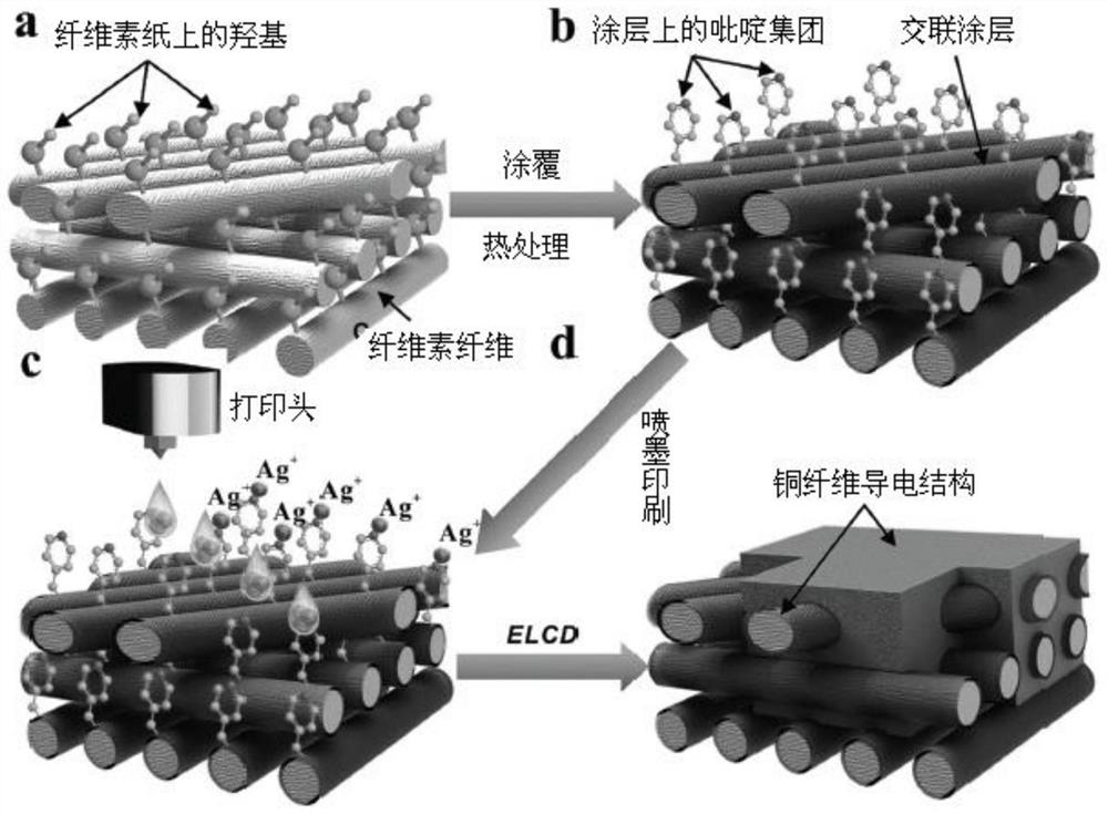
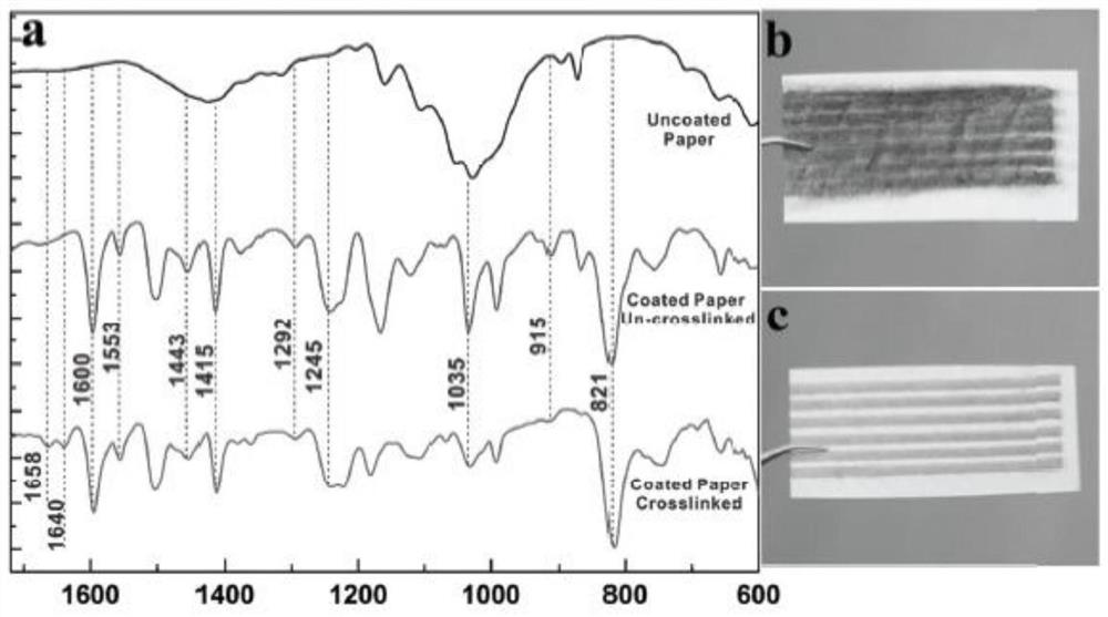
[0035] Example 1: Surface modification of porous substrates

[0036] Untreated cellulose paper was dipped directly into the coating solution for 5 seconds. The paper was then slowly drawn out of the solution and allowed to air dry for 5 minutes at room temperature. Finally, the coated paper was placed in an oven at 135 °C for 20 minutes for the in situ cross-linking reaction of SU-8 and P4VP molecules.

Embodiment 2

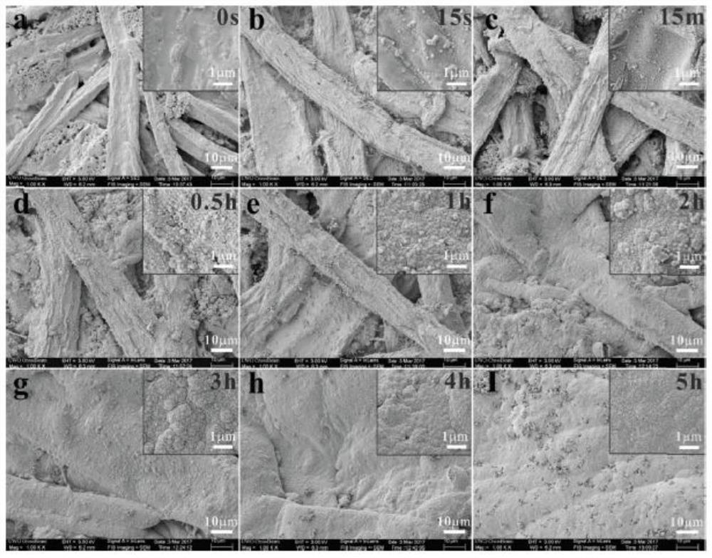
[0037] Example 2: Fabrication of High Conductivity Circuit

[0038] Glycerol-water solution was prepared by mixing anhydrous glycerol and distilled water at a volume ratio of 3:2. Silver nitrate was then added followed by mixing in a VWR mixer for 4 minutes to form a 60 mg / mL silver salt solution. The prepared ink was degassed in a vacuum chamber at 2 psi for 1 hour to remove dissolved gases and air bubbles. The viscosity and surface tension of the final ink were 11.5 cp and 53.5 mN / m, respectively. These values ​​are within the optimum range for the Dimatix DMP-2800 printer. Use a 0.2 μm nylon syringe filter to remove unwanted particles from the ink. Ink is loaded into a cartridge mounted on a 10pL piezoelectric drop-of-drop (DOD) inkjet printhead. The printing parameters are set as: drop distance, 30 μm; meniscus vacuum degree, 3.5 inches H 2 O column; print head temperature, 25°C; print head angle, 4.2°; jetting voltage, 25.1V. Printing was performed at room temperatu...

Embodiment 3

[0039] Embodiment 3: the making of non-drilling multilayer circuit

[0040] As in Example 2, the ink was loaded into a cartridge mounted on a 10 pL piezoelectric drop-of-drop (DOD) inkjet printhead. The printing parameters are set as: drop distance, 30 μm for conventional circuit, 5 μm for through hole; vacuum degree of meniscus, 3.5 inches H 2 O column; print head temperature, 25°C; print head angle, 4.2°; jetting voltage, 25.1V. Smaller droplet spacing can cause an increase in ink volume per unit area, so ink will penetrate more into the porous substrate rather than remain on the surface. By controlling the volume of ink per unit area, the depth of penetration can be finely tuned in the treated porous substrate so that the substrate can be metallized at the desired depth. For the interconnection between layers, we use a small droplet pitch (4 ·5H 2 O (14g / L), NaOH (12g / L), potassium sodium tartrate (16g / L), EDTA·2Na (20g / L), HCHO (26mL / L), 2,2'-bipyridine (20mg / L ) and p...


PUM

PropertyMeasurementUnit
thicknessaaaaaaaaaa
frequencyaaaaaaaaaa

Abstract

The present invention discloses efficient fabrication of single-layer and multi-layer circuits with highly conductive connections without drilling, in particular, on low-cost porous substrates with strong adhesion and enhanced bending durability and in one-step drilling-free Method for producing copper-fiber mixtures with high conductive properties on metal-deposited low-cost porous substrates, and products made according to said method. The invention uses a one-step dip coating method to modify the surface of the porous medium, and uses ink-jet printing and silver ion-catalyzed ELD to selectively metallize the substrate surface. Due to the abundant pyridine ligands on the substrate surface, the modified substrate exhibits strong and reliable binding to deposited copper during the ELD process. In addition, the unique porous structure allows its fibers to act as physical anchors, resulting in copper-fiber conductive structures. This reinforced structure not only prevents the delamination of the copper film but also improves its bending durability. The present invention also enables highly conductive copper layers with low sheet resistance on porous substrates without significant loss of resolution.

Description

technical field [0001] The invention belongs to the technical field of printed electronics, and more specifically relates to printed electronic products on porous substrates. Background technique [0002] Over the past decade, printed electronics (PE) technology has gained considerable attention to exploit existing printing industry manufacturing capabilities to produce circuits cheaply and efficiently. This dynamic new technology is transforming the electronics industry by replacing traditional and costly methods of manufacturing electronic components, devices and even systems. Increasingly, printed thin-film transistors, conductors, inductors, and capacitors are being integrated with electronics to develop new types of systems, such as thin-film energy harvesting / storage systems, smart labels, radio-frequency identification (RFID) tags, and storage devices. In the near future, it is foreseeable that flexible, wearable, and even stretchable devices realized by printing tec...

Claims


Application Information

Patent Timeline
Patent Type & Authority Patents(China)
IPC IPC(8): H05K3/12H05K3/18H05K1/09
CPCH05K1/09H05K3/125H05K3/181H05K2203/013H05K2201/0281H05K1/189H05K3/182H05K2201/0116H05K2201/0154H05K2201/10098H05K2201/10106H05K2203/0709H05K2203/1361C23C18/1644C23C18/2086C23C18/285C23C18/30C23C18/405H05K1/0393H05K3/387H05K1/0386H05K2203/072H05K3/425H05K2203/166H05K3/429H05K3/422H05K1/092C23C18/166C23C18/165C23C18/1692
Inventor 杨军张腾元郭秋泉
Owner 杨军
Why Eureka
Try Eureka