Supercharge Your Innovation With Domain-Expert AI Agents!

A large-area thick film for gan neutron detectors 6 Preparation method of lif neutron conversion layer

A neutron detector, large-area technology, used in semiconductor detector measurement, coating, ion implantation plating, etc. problem, to achieve the effect of high neutron detection efficiency, high sensitivity and good crystal quality

Active Publication Date: 2020-06-30
EAST CHINA UNIV OF TECH
View PDF8 Cites 0 Cited by
  • Summary
  • Abstract
  • Description
  • Claims
  • Application Information

AI Technical Summary

Problems solved by technology

[0003] The object of the present invention is aimed at the existing GaN neutron detector 6 The area and film thickness of the Li neutron conversion layer cannot meet the requirements, and there are deficiencies in aspects such as easy falling off or cracking. The invention provides a large-area thick film used in a GaN neutron detector. 6 LiF neutron conversion layer preparation method

Method used


Image

  • A large-area thick film for gan neutron detectors  <sup>6</sup> Preparation method of lif neutron conversion layer
  • A large-area thick film for gan neutron detectors  <sup>6</sup> Preparation method of lif neutron conversion layer
  • A large-area thick film for gan neutron detectors  <sup>6</sup> Preparation method of lif neutron conversion layer

Examples


Embodiment 1

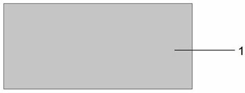
[0034] First, a GaN self-supporting substrate 1 with a thickness of 100 μm was placed in a 120-degree H 2 SO 4 :H 2 o 2 (5:1) Boil in the mixed solution for 5 minutes, then soak in the HCL:DI=3:1 mixed solution for 5 minutes to remove the oxides on the GaN surface; then use acetone, isopropanol, deionized GaN substrate Water was ultrasonically cleaned for 5 minutes each to remove organic and inorganic contamination on the GaN surface, and then dried with nitrogen gas with a purity of 99.999% ( figure 2 );

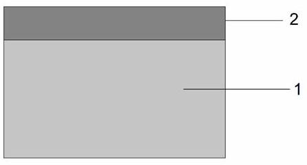
[0035] Secondly, put the cleaned GaN substrate into the electron beam evaporation equipment and evacuate to 8×10 -6 pa, deposit Au with a thickness of 1 μm on the front surface of the GaN substrate to form the front Au electrode 2 ( image 3 );

[0036]Subsequently, a layer of negative photoresist 3 ( Figure 4 ), the first rotation speed of the homogenizer is 500 rpm, and the time is 8 seconds; the second rotation speed is 2500 rpm, and the time is 20 seconds; then...

Embodiment 2

[0040] First, a GaN self-supporting substrate 1 with a thickness of 100 μm was placed in a 120-degree H 2 SO 4 :H 2 o 2 (5:1) Boil in the mixed solution for 5 minutes, then soak in the HCL:DI=3:1 mixed solution for 5 minutes to remove the oxides on the GaN surface; then use acetone, isopropanol, deionized GaN substrate Water was ultrasonically cleaned for 5 minutes each to remove organic and inorganic contamination on the GaN surface, and then dried with nitrogen gas with a purity of 99.999% ( figure 2 );

[0041] Secondly, put the cleaned GaN substrate into the electron beam evaporation equipment and evacuate to 8×10 -6 pa, deposit Au with a thickness of 0.8 μm on the front surface of the GaN substrate to form the front Au electrode 2 ( image 3 );

[0042] Subsequently, a layer of negative photoresist 3 ( Figure 4 ), the first speed of the homogenizer is 500 rpm for 8 seconds, the second speed is 3000 rpm for 20 seconds; then put it on a hot plate at 90°C for 90 sec...

Embodiment 3

[0046] First, a GaN self-supporting substrate 1 with a thickness of 100 μm was placed in a 120-degree H 2 SO 4 :H 2 o 2 (5:1) Boil in the mixed solution for 5 minutes, then soak in the HCL:DI=3:1 mixed solution for 5 minutes to remove the oxides on the GaN surface; then use acetone, isopropanol, deionized GaN substrate Water was ultrasonically cleaned for 5 minutes each to remove organic and inorganic contamination on the GaN surface, and then dried with nitrogen gas with a purity of 99.999% ( figure 2 );

[0047] Secondly, put the cleaned GaN substrate into the electron beam evaporation equipment and evacuate to 8×10 -6 pa, deposit Au with a thickness of 2 μm on the front surface of the GaN substrate to form the front Au electrode 2 ( image 3 );

[0048] Subsequently, a layer of negative photoresist 3 ( Figure 4 ), the first rotation speed of the homogenizer is 500 rpm, and the time is 8 seconds; the second rotation speed is 2000 rpm, and the time is 20 seconds; the...


PUM

PropertyMeasurementUnit
thicknessaaaaaaaaaa
thicknessaaaaaaaaaa
thicknessaaaaaaaaaa

Abstract

The invention discloses a large-area thick film <6>LiF neutron conversion layer preparation method for a GaN neutron detector. The large-area thick film <6>LiF neutron conversion layer preparation method comprises the steps that a GaN substrate is subjected to surface treatment; Au is deposited on the front surface of GaN to form a front Au electrode; a pit-type GaN patterned Au electrode is obtained by utilizing photolithography technique and wet etching; the pit-type GaN patterned Au electrode is placed in a vacuum coating device and the GaN substrate is heated; and in the earlier stage of evaporation, low-speed evaporation of <6>LiF is performed, and in the later stage, high-speed evaporation of a <6>LiF neutron conversion layer meeting the thickness requirements is performed. The large-area thick film <6>LiF neutron conversion layer for the GaN neutron detector prepared by the large-area thick film <6>LiF neutron conversion layer preparation method has the advantages of large areaand thick film for preparing the conversion layer, good crystal quality, no falling off, high neutron detection efficiency and high sensitivity, and has important application value in aerospace exploration, nuclear energy utilization and development, production and application of radioisotopes, and multiple special fields.

Description

technical field [0001] The invention relates to the technical field of neutron detection, especially the need to prepare large-area and thick films 6 Thin film preparation method of LiF neutron conversion layer. Background technique [0002] The nuclear reaction method uses neutrons to react with matter to generate charged particles and then detects charged particles, which has certain advantages in the detection of semiconductor neutrons. In the current neutron detection technology, the semiconductor neutron detector prepared by nuclear reaction method detects neutrons, and its essence is neutrons and certain substances (such as 6 Li, 10 B) The new product after the nuclear reaction contains charged particles. After the charged particles enter the semiconductor material, they ionize the outer electrons in the material, thereby generating electron-hole pairs, thereby realizing the detection of neutrons. Gallium Nitride (GaN), as the third-generation wide-band gap straight...

Claims


Application Information

Patent Timeline
Patent Type & Authority Patents(China)
IPC IPC(8): C23C14/18C23C14/30C23C14/58C23C14/06G01T3/08
CPCC23C14/0694C23C14/18C23C14/30C23C14/5873G01T3/08
Inventor 朱志甫邹继军汤彬黄河彭新村
Owner EAST CHINA UNIV OF TECH
Features
  • R&D
  • Intellectual Property
  • Life Sciences
  • Materials
  • Tech Scout
  • Unparalleled Data Quality
  • Higher Quality Content
  • 60% Fewer Hallucinations
Learn More