A semiconductor diode electroplating processing system

A technology of electroplating treatment and diodes, which is applied in the direction of semiconductor devices, circuits, electrolytic components, etc., can solve the problems of affecting the efficiency and quality of electroplating, inability to electroplating, bubble treatment, etc., to improve the efficiency and quality of electroplating, improve efficiency and quality, Increase the effect of contact

Active Publication Date: 2019-08-13
吉林瑞能半导体有限公司
View PDF1 Cites 2 Cited by
  • Summary
  • Abstract
  • Description
  • Claims
  • Application Information

AI Technical Summary

Problems solved by technology

However, the technical solution cannot perform electroplating quickly and cannot deal with the bubbles remaining in the electroplating solution, which affects the efficiency and quality of electroplating
making the technical solution limited

Method used


Image

  • A semiconductor diode electroplating processing system
  • A semiconductor diode electroplating processing system
  • A semiconductor diode electroplating processing system

Examples


Embodiment approach

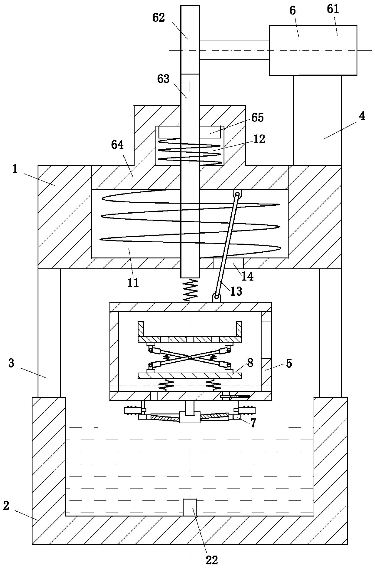
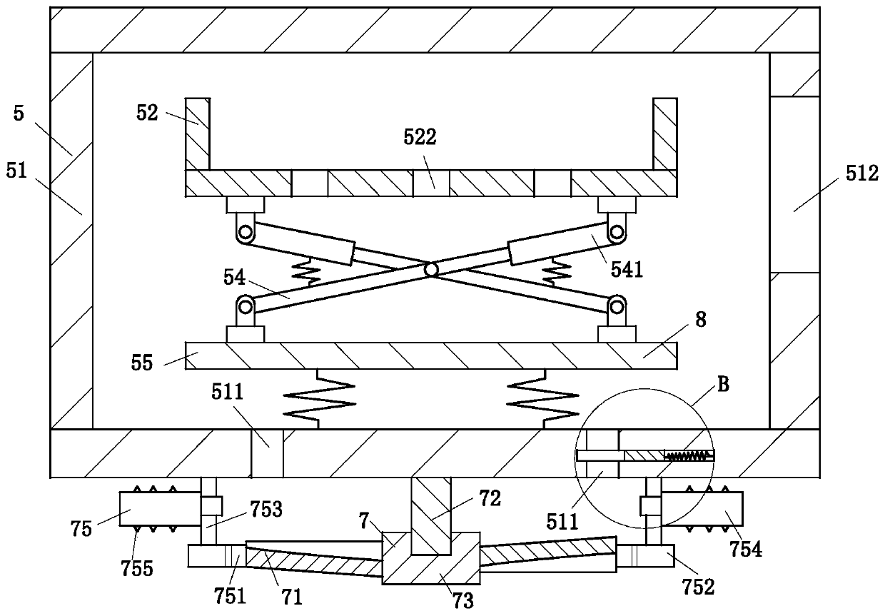
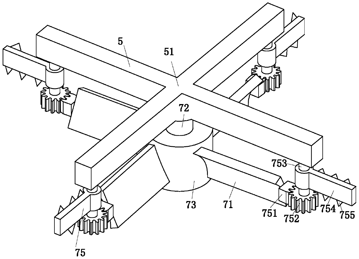
[0026] As an embodiment of the present invention, the electroplating box 5 is provided with a swing module 8 inside, and the electroplating box 5 includes a box body 51, a support plate 52, a vibrating frame 54 and a No. 4 plate 55; the top of the box body 51 The No. 3 spring is fixedly connected with the No. 1 sliding telescopic rod 63, and the bottom of the box body 51 is provided with two No. 1 liquid inlets 511, and the side wall of the box body 51 is provided with an opening and closing door 512; the No. 4 plate 55 passes through The No. 4 spring is fixedly installed at the bottom of the casing 51; the vibrating frame 54 is made up of two No. 1 telescopic rods 541; One end of the No. 1 telescopic rod 541 is hinged at the top of No. 4 plate 55, and the other end of the No. 1 telescopic rod 541 is hinged at the bottom of the support plate 52; the bottom of the support plate 52 is provided with a No. 2 liquid inlet 522, and the support The plate 52 is used to store semicondu...


PUM


Abstract

The invention belongs to the technical field of semiconductor diode production, and particularly relates to a semiconductor diode electroplating treatment system. The semiconductor diode electroplating treatment system comprises a top plate, an electroplating bath, a supporting column, an electroplating tank, a drive module and a stirring module; the drive module comprises a first motor, a first cam, a first sliding telescopic rod, a first sliding block, and a second sliding block, through cooperation of the first cam, the first sliding block and the first sliding telescopic rod, the electroplating tank swings while descending, electroplating liquid makes sufficient contact with the semiconductor diode, a third sliding block plugs a first liquid inlet in the right side, the electroplatingliquid enters from the first liquid inlet in the left side of a bottom plate of a tank body and impacts a fourth plate, a supporting disc on the fourth plate shakes, the electroplating liquid enters the electroplating tank, through vibration of a vibration frame, the semiconductor diode vibrates, the contact area between the electroplating liquid and the semiconductor diode can be increased, and the electroplating efficiency and the quality of the semiconductor diode are improved.

Description

technical field [0001] The invention belongs to the technical field of semiconductor diode production, in particular to a semiconductor diode electroplating treatment system. Background technique [0002] A diode is an electronic component, a device with two electrodes that only allows current to flow in one direction. The most common function of a diode is to only allow current to pass in a single direction (called forward bias), and to block it when it is reversed (called reverse bias). So a diode can be thought of as the electronic version of a check valve. [0003] Diode lead electroplating machine has methods such as barrel plating and rack plating. Plating is suitable for electroplating of small parts that cannot be or are not suitable for hanging due to factors such as shape and size. It adopts rack plating or basket plating for early small parts electroplating. Compared with it, it saves labor, improves labor production efficiency, and greatly improves the surface ...

Claims


Application Information

Patent Timeline
Patent Type & Authority Patents(China)
IPC IPC(8): C25D17/18C25D5/20C25D7/12C25D21/10
CPCC25D5/20C25D7/12C25D17/18C25D21/10
Inventor 陈涛
Owner 吉林瑞能半导体有限公司
Why Eureka
Try Eureka