Plating apparatus and method of manufacturing printed circuit board

A technology for electroplating devices and substrates, which is applied in the manufacture of printed circuits, printed circuits, electrodes, etc., and can solve problems such as the current reduction of anode electrodes

Inactive Publication Date: 2011-07-20
NITTO DENKO CORP
View PDF1 Cites 6 Cited by
  • Summary
  • Abstract
  • Description
  • Claims
  • Application Information

AI Technical Summary

Problems solved by technology

Therefore, sometimes the current flowing to a part of the anode electrode becomes significantly smaller
Therefore, efficient plating cannot be performed

Method used


Image

  • Plating apparatus and method of manufacturing printed circuit board
  • Plating apparatus and method of manufacturing printed circuit board
  • Plating apparatus and method of manufacturing printed circuit board

Examples


no. 2 Embodiment approach

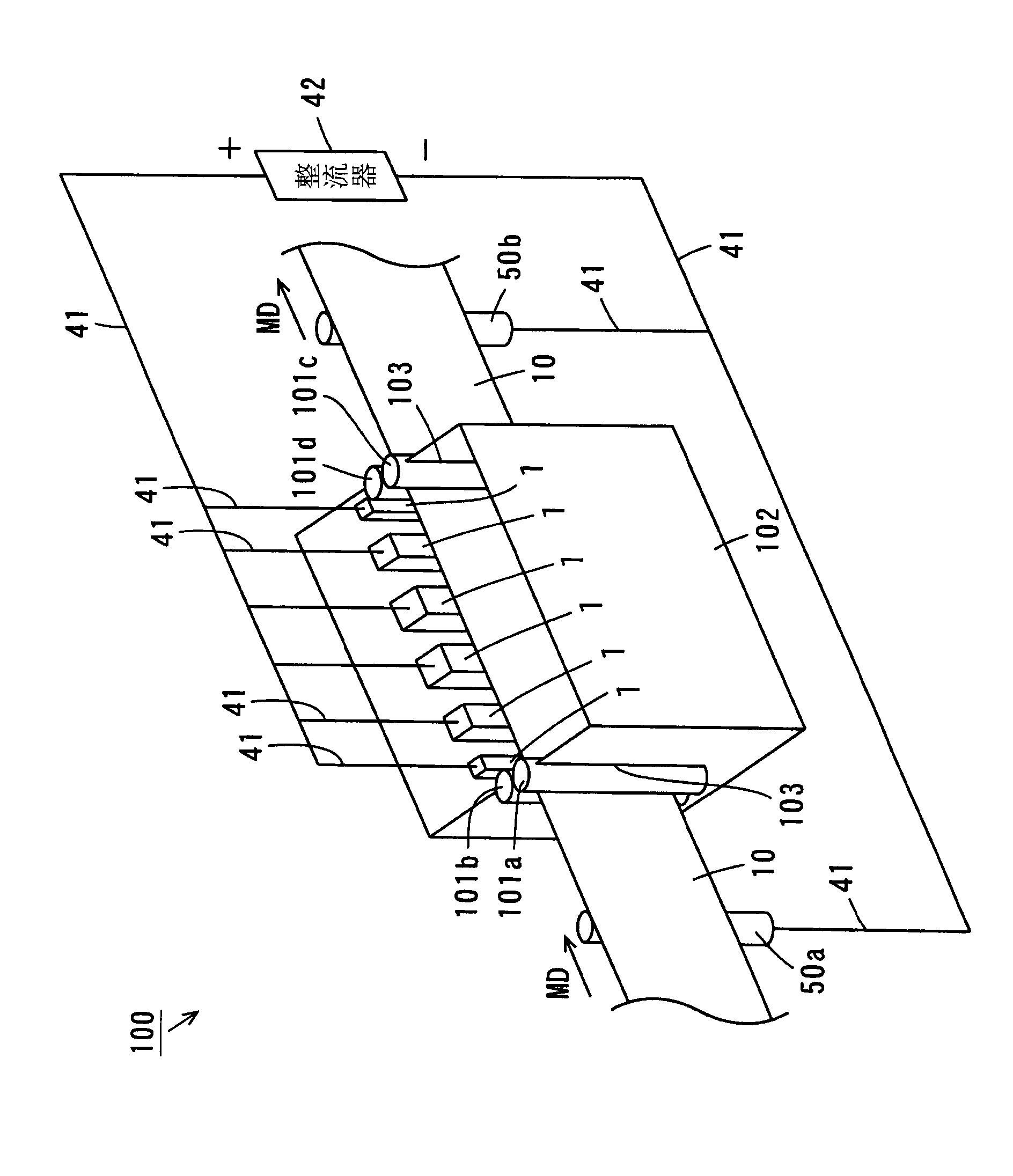
[0062] Regarding the electroplating apparatus 100 of the second embodiment of the present invention, differences from the electroplating apparatus 100 of the above-mentioned first embodiment will be described.

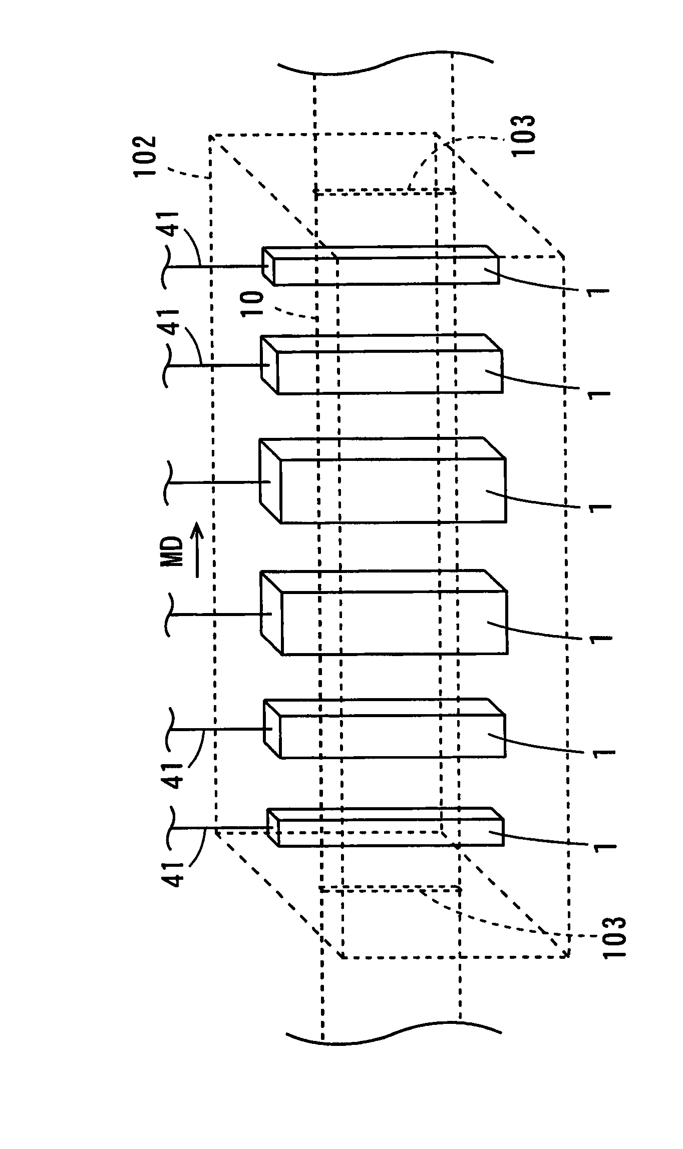
[0063] Figure 4 It is a figure which shows the structure of the some anode electrode 2 of the electroplating apparatus 100 of 2nd Embodiment. Such as Figure 4 As shown, the plating apparatus 100 of the second embodiment has three or more (six in this example) anode electrodes 2 instead of three or more anode electrodes 1 . Each anode electrode 2 has a structure in which a plurality of spherical anode balls 112 made of, for example, copper are accommodated in a mesh-shaped case 110 made of, for example, titanium. Each anode electrode 2 is placed in the plating tank 102 in a state of being accommodated in an acid-resistant anode cover 113 .

[0064] Hereinafter, among the plurality of anode electrodes 2, the two anode electrodes 2 disposed at both ends are respectiv...

Embodiment 2 and Embodiment 3

[0082] In Example 2 and Example 3, the plating apparatus 100 of the above-mentioned second embodiment was used. In embodiment 2, adopt the anode ball 112 that diameter is 27mm, make the quantity of the anode ball 112 of each two ends anode 2 be 25, make the quantity of the anode ball 112 of each middle anode 2 be 45, make each central anode The number of anode balls 112 is 80. In embodiment 3, adopt the anode ball 112 that diameter is 27mm, make the quantity of the anode ball 112 of each two-end anode 2 be 25, make the anode of the intermediate anode 2 on the upstream side on the transport direction of the elongated substrate 10 The number of balls 112 is 45, the number of anode balls 112 of the intermediate anode 2 on the downstream side in the transport direction of the elongated substrate 10 is 50, and the number of anode balls 112 of each central anode 2 is 80.


PUM

PropertyMeasurementUnit
surface areaaaaaaaaaaa

Abstract

The invention provides a plating apparatus and a method of manufacturing printed circuit board. The plating apparatus includes a plating tank. The plating tank contains a plating solution. A long-sized substrate is transported by transport rollers to pass through inside of the plating tank. Three or more bar-shaped anodes are provided in the plating tank to line up along the long-sized substrate. A surface area of each of the anodes arranged at both ends is smaller than a surface area of another anode.

Description

technical field [0001] The present invention relates to a method for manufacturing an electroplating device and a wired circuit board. Background technique [0002] In recent years, higher-density and smaller-sized printed circuit boards have been used in various electronic devices. When manufacturing a wired circuit board, for example, in a step of forming a wiring pattern, electrolytic plating is performed on a previously formed seed layer using a plating apparatus. [0003] For example, the electroplating apparatus described in JP-A-2003-321796 has an electroplating tank containing an electroplating solution. An anode electrode is arranged in the electroplating tank. The elongated substrate is conveyed into the plating tank through the slit formed in the side wall of the plating tank. In this state, a voltage is applied between the anode electrode and the region to be electrolytically plated on the elongated substrate. Thus, electrolytic plating is performed on the el...

Claims


Application Information

Patent Timeline
Patent Type & Authority Applications(China)
IPC IPC(8): C25D7/00C25D17/00
CPCC25D21/00H05K3/18C25D7/0642C25D7/0621C25D7/06C25D17/00C25D7/00C25D17/12
Inventor 西胁谦一郎
Owner NITTO DENKO CORP
Why Eureka
Try Eureka