A graphene hybrid plasmonic modulator based on a buried silicon waveguide

A silicon waveguide and buried technology, applied in the field of graphene optoelectronic modulators, can solve the problems of low transmission loss and inability to achieve high modulation depth

Active Publication Date: 2021-09-10
SOUTHEAST UNIV
View PDF4 Cites 0 Cited by
  • Summary
  • Abstract
  • Description
  • Claims
  • Application Information

AI Technical Summary

Problems solved by technology

[0005] The purpose of the present invention is to overcome the deficiencies of the prior art, provide a graphene hybrid plasmonic modulator based on buried silicon waveguide, and solve the problem that the existing optical modulator cannot achieve high modulation depth while ensuring low transmission loss

Method used


Image

  • A graphene hybrid plasmonic modulator based on a buried silicon waveguide
  • A graphene hybrid plasmonic modulator based on a buried silicon waveguide
  • A graphene hybrid plasmonic modulator based on a buried silicon waveguide

Examples


Embodiment Construction

[0021] Embodiments of the present invention will be described below in conjunction with the accompanying drawings.

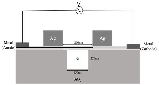
[0022] Such as figure 1 As shown, the present invention designs a graphene hybrid plasmonic modulator based on a buried silicon waveguide, including a hybrid plasmonic waveguide and a graphene sandwich structure, wherein the hybrid plasmonic waveguide consists of two silver waveguides and a buried silicon waveguide. The modulator is composed of 6 layers, from top to bottom are two silver plasmonic waveguides, an alumina isolation layer, a graphene sandwich structure, an alumina isolation layer, a buried silicon waveguide, and a silicon dioxide substrate. The graphene sandwich structure consists of an upper single-layer graphene, an intermediate alumina isolation medium and a lower single-layer graphene. And, the upper and lower single-layer graphene are respectively in contact with the left and right metal electrodes, and the upper and lower single-layer graphe...


PUM

PropertyMeasurementUnit
heightaaaaaaaaaa
widthaaaaaaaaaa

Abstract

The invention discloses a graphene hybrid plasma modulator based on buried silicon waveguide, which comprises a hybrid plasma waveguide and a graphene sandwich structure, wherein the hybrid plasma waveguide consists of two silver waveguides and one buried silicon waveguide. The modulator is composed of 6 layers, from top to bottom, there are two silver plasma waveguides, an alumina isolation layer, a graphene sandwich structure, an alumina isolation layer, a buried silicon waveguide, and a silicon dioxide substrate. The graphene sandwich structure consists of an upper single-layer graphene, an intermediate alumina isolation medium and a lower single-layer graphene. And, the upper and lower single-layer graphenes are respectively in contact with the left and right metal electrodes, and the upper and lower single-layer graphenes are turned on and off of the light modulator under the action of electric signals from the left and right metal electrodes. The invention can realize optical modulation with high modulation depth, low transmission loss and high modulation bandwidth, and can be applied in integrated high-speed all-optical networks.

Description

technical field [0001] The invention relates to a hybrid plasmonic waveguide technology based on a buried silicon waveguide, and belongs to the technical field of graphene photoelectric modulators. Background technique [0002] Optical modulators are key to high-speed, short-distance optical communications. At present, optical modulators are developing towards higher speed, wider bandwidth, smaller device size and integration. Traditional modulators can no longer keep up with the development of optical fiber communication. Research to develop new modulators is imminent. [0003] Graphene is a two-dimensional carbon nanomaterial in which carbon atoms form a hexagonal honeycomb lattice with sp² hybrid orbitals. Due to its excellent electrical and optical properties, it has attracted widespread interest. Graphene has extremely high electron mobility and can be used to make high-efficiency light modulators. [0004] Graphene can be combined with high-refractive index dielectr...

Claims


Application Information

Patent Timeline
Patent Type & Authority Patents(China)
IPC IPC(8): G02F1/00G02F1/01
CPCG02F1/0018G02F1/0063G02F1/0102G02F1/011
Inventor 胡国华朱渊恽斌峰张若虎崔一平
Owner SOUTHEAST UNIV
Why Eureka
Try Eureka