Graphene mixed plasma modulator based on buried silicone waveguide
A silicon waveguide, buried technology, applied in the field of graphene optoelectronic modulators, can solve the problems of low transmission loss, inability to achieve high modulation depth, etc., and achieve the effects of low transmission loss, high modulation bandwidth, and high modulation depth
- Summary
- Abstract
- Description
- Claims
- Application Information
AI Technical Summary
Problems solved by technology
Method used
Image
Examples
Embodiment Construction
[0021] The embodiments of the present invention will be described below in conjunction with the accompanying drawings of the specification.
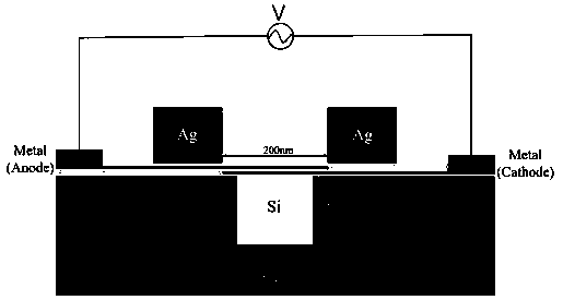
[0022] Such as figure 1 As shown, the present invention designs a graphene hybrid plasma modulator based on a buried silicon waveguide, which includes a hybrid plasma waveguide and a graphene sandwich structure, where the hybrid plasma waveguide is composed of two silver waveguides and a buried silicon waveguide. The modulator consists of a 6-layer structure. From top to bottom, there are two silver plasma waveguides, an alumina isolation layer, a graphene sandwich structure, an alumina isolation layer, a buried silicon waveguide, and a silica substrate. The graphene sandwich structure is composed of an upper single-layer graphene, an intermediate alumina isolation medium, and a lower single-layer graphene. And, the upper and lower single-layer graphene respectively contact the left and right metal electrodes, and the upper and lower single...
PUM
 Abstract
Description
Claims
Application Information


