Silicon carbide gate-turn-off thyristor and manufacturing method thereof

A silicon carbide gate and thyristor technology, which is used in semiconductor/solid-state device manufacturing, electrical components, circuits, etc., can solve the problem of poor resistance to dV/dt, uneven distribution of on-state dynamic current, and poor resistance to dI/dt. and other problems, to achieve the effect of improving the ability to resist dI/dt and dV/dt, reducing the current density of the collector and enhancing the reliability

Active Publication Date: 2018-11-23
HANGZHOU UG MIN SEMICON TECH CO LTD
View PDF3 Cites 3 Cited by
  • Summary
  • Abstract
  • Description
  • Claims
  • Application Information

AI Technical Summary

Problems solved by technology

[0005] Compared with voltage-driven transistor SiC MOS tube and SiC IGBT, SiC GTO has the advantages of low cost, high power and easy fabrication. However, SiC GTO in the prior art has two major weaknesses that have not been overcome.
One is that the ability to resist dI / dt is poor, requiring complex limiting circuits
The other is the poor ability to resist dV / dt, which requires complex absorption circuits
[0006] Wang Jun of Hunan University and others published "SiC GTO Thyristor Technology Status and Development" in the 7th issue of 2016 "High Power Conversion Technology". GTO has made great progress, but there have always been problems limited by di / dt and dv / di, which cannot be solved internally
The article pointed out: "SiC GTO also has some disadvantages: the dynamic current distribution is uneven, a buffer that limits di / dt is required at the moment of turn-on, and its reverse bias safe operating area (RBSOA) is relatively small; the PNPN structure of SiC GTO Making the GTO sensitive to dv / dt changes may cause false turn-on, so a du / dt-limiting snubber is also needed at turn-off
When the current density at a point near the emitter area of ​​the upper tube increases so that α1+α2=1 at this point, the point turns from cut-off to conduction, which causes the failure of the entire SiC GTO, and the peripheral current of the emitter area of ​​the upper tube Density also constitutes a limit to the dV / dt of SiC GTO

Method used


Image

  • Silicon carbide gate-turn-off thyristor and manufacturing method thereof
  • Silicon carbide gate-turn-off thyristor and manufacturing method thereof
  • Silicon carbide gate-turn-off thyristor and manufacturing method thereof

Examples


Embodiment Construction

[0050] The specific implementation manner of the present invention will be described in detail below in conjunction with the accompanying drawings and examples.

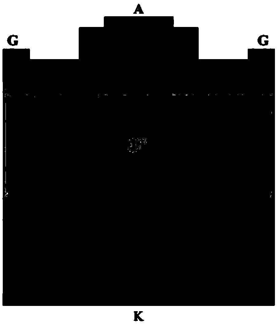
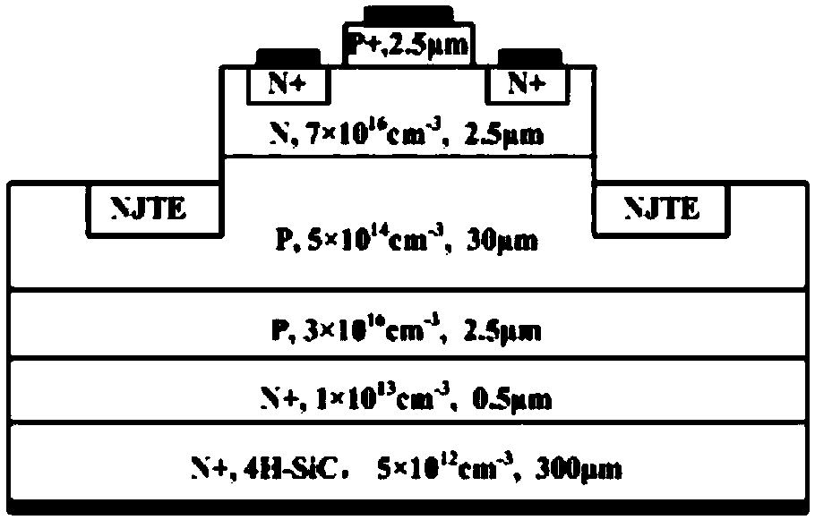
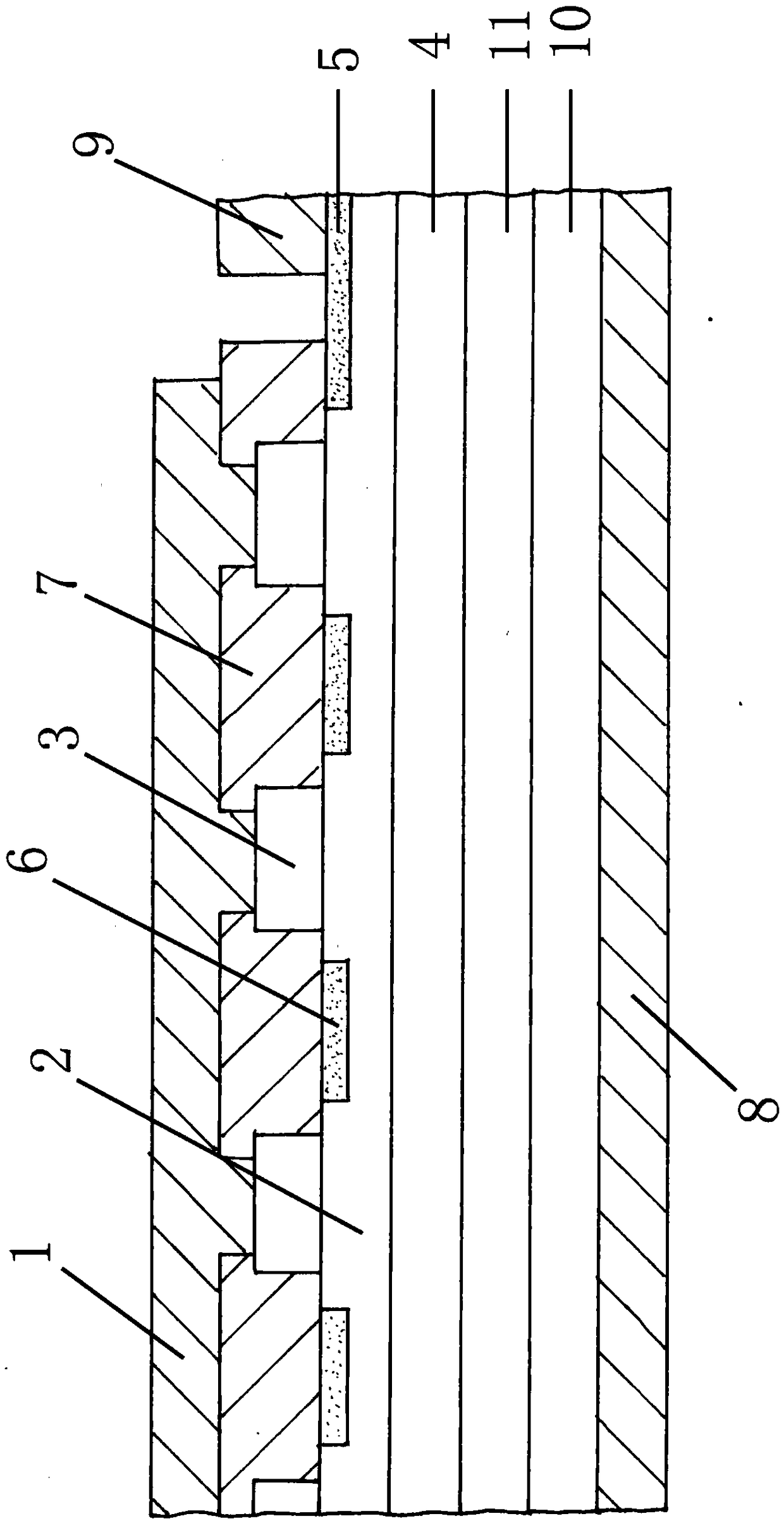
[0051] First of all, the shape of the P-type emission area of ​​the upper tube of the present invention can be rectangular, square, hexagonal, circular, trapezoidal, triangular or other shapes, as well as graphics of various combinations of shapes, usually a rectangle. For the sake of simplicity, many descriptions in the specification use a rectangle for the P-type emitter region, a rectangle for the N-type base region, and a rectangle for the N-type base concentration region. This is an interdigitated structure of a common power transistor.

[0052] Secondly, the mask pattern mentioned in the present invention refers to the GDS pattern of the mask. This is the norm in the industry. To make the mask plate, first use computer-aided design to make the GDS data tape of the graphic generator, and draw the GDS graphics ...


PUM

PropertyMeasurementUnit
lengthaaaaaaaaaa
thicknessaaaaaaaaaa

Abstract

The invention provides a silicon carbide gate-turn-off thyristor. The thyristor is of a PNPN four-layer SiC structure which is arranged on an N+ type SiC substrate; the upper layer is a strip composedof a plurality of repeatedly-arranged upper tube P-type emission regions; the middle layer is composed of an upper tube N-type base region, an upper tube N type thick base region and an upper tube Ntype thick base region bus bar; the upper tube N type thick base region and the upper tube N type thick base region bus bar are crossed or parallel; and the upper surface of the upper tube N-shaped bus bar is connected with a gate pole metal layer. By virtue of the silicon carbide gate-turn-off thyristor provided by the invention, the current density of the periphery can be reduced, and the anti-dI/dt and anti-dV/dt capability can be improved.

Description

technical field [0001] The invention belongs to the technical field of compound semiconductor current-mode power devices, and relates to a silicon carbide gate turn-off thyristor (SiC GTO (Gate-Turn-Off Thyristor)). Background technique [0002] Compound semiconductor material SiC has great advantages over single semiconductor material Si. In recent years, with the maturity of SiC single crystal rod material and epitaxy technology, silicon carbide gate turn-off thyristor (SiC GTO) has been supplied to the market. [0003] figure 1 and figure 2 It is a schematic structural diagram of SiC GTO in the prior art. [0004] SiC GTO is a PNPN four-layer structure, which can be regarded as composed of two bipolar transistors, a PNP upper transistor and an NPN lower transistor. The P-type emitter region of the PNP upper tube is connected to the anode metal layer A. The N-type base area of ​​the PNP upper tube is the N-type collector area of ​​the NPN lower tube. The N-type base ...

Claims


Application Information

Patent Timeline
Patent Type & Authority Applications(China)
IPC IPC(8): H01L29/745H01L21/332H01L29/06
CPCH01L29/0661H01L29/66363H01L29/745
Inventor 李思敏
Owner HANGZHOU UG MIN SEMICON TECH CO LTD
Why Eureka
Try Eureka