Organic thin film transistor

一种有机薄膜、晶体管的技术,应用在有机薄膜晶体管领域,能够解决影响、有机薄膜晶体管电性稳定性不利等问题,达到提升电性稳定性、均匀厚度的效果

Active Publication Date: 2018-11-23
E INK HLDG INC
View PDF8 Cites 0 Cited by
  • Summary
  • Abstract
  • Description
  • Claims
  • Application Information

AI Technical Summary

Problems solved by technology

In other words, the non-uniform thickness of the semiconductor layer will adversely affect the electrical stability of the organic thin film transistor

Method used


Image

  • Organic thin film transistor
  • Organic thin film transistor
  • Organic thin film transistor

Examples


Embodiment Construction

[0021] A number of implementations of the present invention will be disclosed below with the accompanying drawings. For the sake of clarity, many practical details will be described together in the following description. It should be understood, however, that these practical details should not be used to limit the invention. That is, in some embodiments of the present invention, these practical details are unnecessary. In addition, for the sake of simplifying the drawings, some well-known and commonly used structures and elements will be shown in a simple and schematic manner in the drawings.

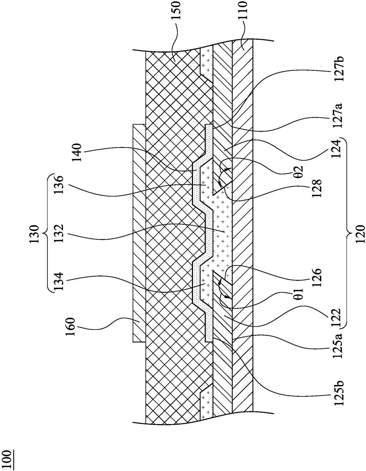
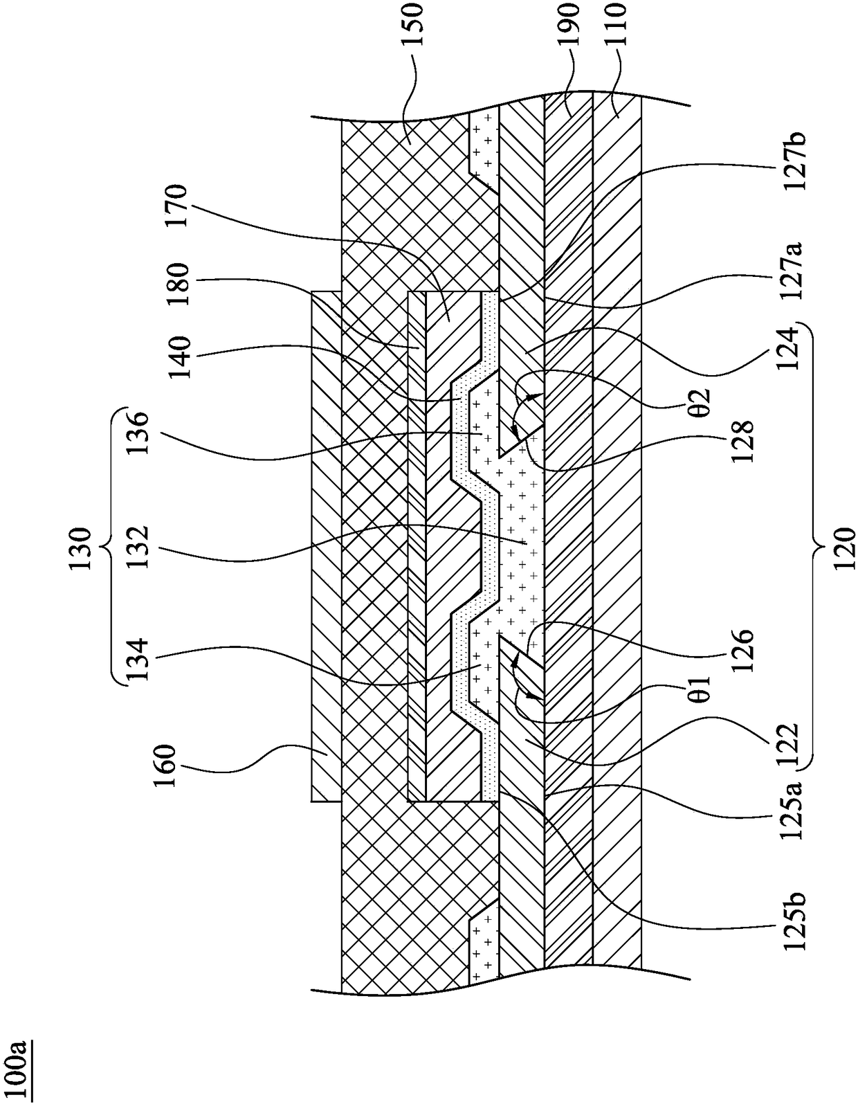
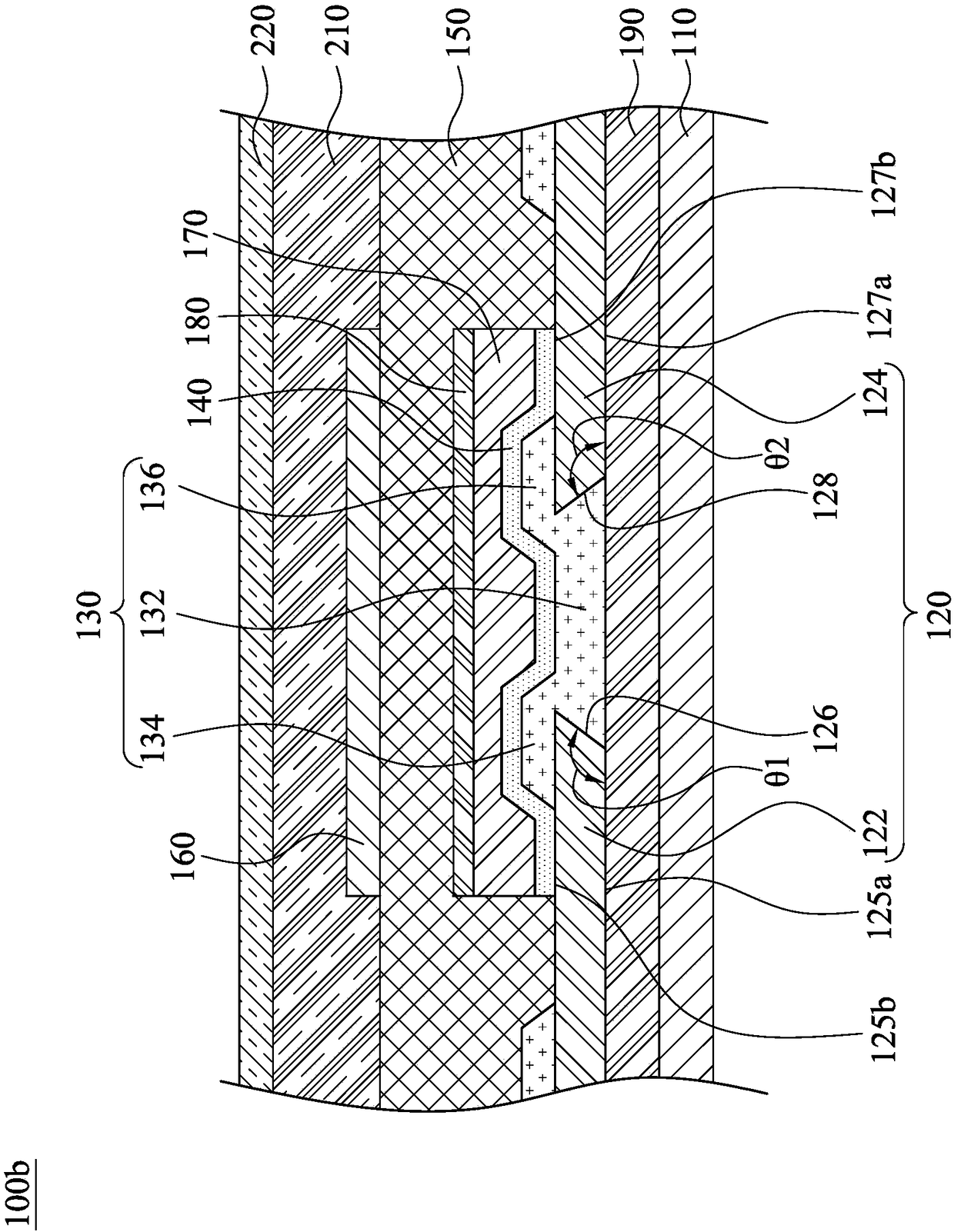
[0022] figure 1 A cross-sectional view of an organic thin film transistor 100 according to an embodiment of the present invention is shown. As shown in the figure, the organic thin film transistor 100 includes a substrate 110 , a source / drain layer 120 , a first buffer layer 130 , a semiconductor layer 140 , a gate insulating layer 150 and a gate 160 . Wherein, the source / drain layer...


PUM


Abstract

The invention discloses an organic thin film transistor, comprising a substrate, a source / drain layer, a first buffer layer, a semiconductor layer, a gate insulating layer, and a gate electrode, wherein the source / drain layer is located on the substrate and has a source region and a drain region; the first buffer layer is located between the source region and the drain region and covers at least part of the source region and at least part of the drain region; the semiconductor layer is located on the source / drain layer and the first buffer layer; the first buffer layer is located among the semiconductor layer, the source region, the drain region, and the substrate; the gate insulating layer covers the source / drain layer and the semiconductor layer; the gate electrode is located on the gateinsulating layer, and part of the gate insulating layer is located between the gate electrode and the semiconductor layer; and the first buffer layer may be used to fill the space between the sourceregion and the drain region to prevent the semiconductor layer from being formed on the wedge undercut structure of the source region and the drain region, so that the semiconductor layer has an eventhickness to improve the electrical stability of the organic thin film transistor.

Description

technical field [0001] The invention relates to an organic thin film transistor. Background technique [0002] Generally speaking, the source / drain layer of an organic thin film transistor is made of gold, silver or other metals that can react with a self-assembled monolayer (SAM), wherein the self-assembled monolayer is an organic film The semiconducting layer of the transistor. [0003] When making an organic thin film transistor, the source / drain layer is first patterned to form a source region and a drain region spaced apart, and then a semiconductor layer is coated on the source region and the drain region close to the distance to be connected to the source. In the space between the region and the drain region. However, limited by the material of the source / drain layer, after the source / drain layer is patterned, a taper undercut structure will be generated at a position close to the distance between the source region and the drain region. In this way, the semiconduct...

Claims


Application Information

Patent Timeline
Patent Type & Authority Applications(China)
IPC IPC(8): H01L51/05H01L51/10
CPCH10K10/46H10K10/80H10K71/12H10K71/621H10K10/474H10K10/464H10K10/484H10K10/84H10K10/88H10K10/471
Inventor 林冠峄唐文忠陈柏炜许毓麟
Owner E INK HLDG INC
Why Eureka
Try Eureka