Gate-turn-off thyristor and manufacturing method thereof

A thyristor and gate technology, applied in the field of gate turn-off thyristors, can solve the problem of large die area, and achieve the effects of low dynamic power consumption, reduced requirements and high production efficiency

Inactive Publication Date: 2018-11-27
HANGZHOU UG MIN SEMICON TECH CO LTD
View PDF0 Cites 2 Cited by
  • Summary
  • Abstract
  • Description
  • Claims
  • Application Information

AI Technical Summary

Problems solved by technology

Die area is too large, only suitable for applications above 1000A
And the thickness of the die is above 350μm, so it is only suitable for applications above 2500V

Method used


Image

  • Gate-turn-off thyristor and manufacturing method thereof
  • Gate-turn-off thyristor and manufacturing method thereof
  • Gate-turn-off thyristor and manufacturing method thereof

Examples


Embodiment Construction

[0061] The content of the present invention will be described below with specific examples.

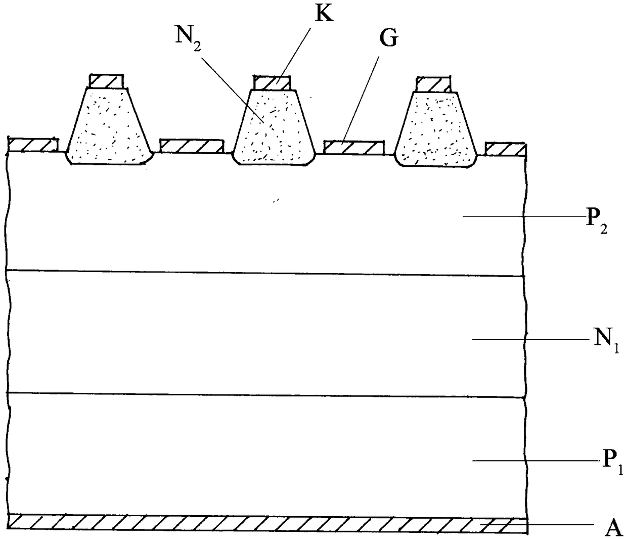
[0062] Firstly, the shape of the N-type emission area of ​​the upper tube of the present invention can be rectangular, square, hexagonal, circular, trapezoidal, triangular or other shapes, and any combination of shapes, usually rectangular. For the sake of brevity, many descriptions in the manual use the rectangular shape of the N-type emission region of the upper tube, the rectangular shape of the P-type base region of the upper tube, and the rectangular shape of the P-type concentrated base region of the upper tube. This is an interdigitated structure of a common power transistor.

[0063] Secondly, the "connection" referred to in the present invention essentially refers to electrical connection, that is, electrical communication. The physical structure can be direct or indirect connection, which does not affect the electrical connection.

[0064] Thirdly, the "repeat distance" me...


PUM


Abstract

The invention provides a gate-turn-off thyristor. A plurality of strips formed by repeatedly arraying a plurality of high-doping-concentration upper tube N type emission regions are arranged on an upper surface of an N type silicon substrate chip; an upper tube P-type concentrated basic region bus bar is arranged around the periphery of each strip; a cathode metal layer is arranged on the upper surface of one upper tube N type emission region, an upper tube P-type basic region is arranged below the upper tube N type emission region, and a side face of the upper tube P-type basic region is connected with an upper tube P-type concentrated basic region or the upper tube P-type concentrated basic region bus bar; an upper tube N-type current collection region is arranged below the upper tube P-type basic region, the upper tube P-type concentrated basic region and the upper tube P-type concentrated basic region bus bar; a lower tube P-type emission region is arranged below the upper tube N-type current collection region; a lower surface of the lower tube P-type emission region is connected with an anode metal layer; a gate metal layer is arranged above the silicon substrate chip. According to the gate-turn-off thyristor provided by the invention, anti-dI/dt ad anti-dV/dt capabilities of turn-off thyristor are remarkably enhanced, and breakdown voltage and a current capacity have a wide application range.

Description

technical field [0001] The invention belongs to the technical field of silicon power devices and relates to a thyristor whose gate can be turned off. Background technique [0002] Gate-turn-off thyristors (Gate-Turn-Off Thyristor, GTO) with silicon as the substrate have been available for more than 50 years. [0003] The structure of the gate-turn-off thyristor in the prior art is as follows figure 1 shown. The gate turn-off thyristor is a PNPN four-layer structure, which can be regarded as composed of two bipolar transistors, namely an NPN upper transistor and a PNP lower transistor. The N-type emission area of ​​the NPN upper tube is N 2 Connect the cathode metal layer K. The P-type base region of the NPN upper tube is the P 2 It is the P-type collector area of ​​the PNP lower tube. NPN upper tube P-type base region P 2 Connect to gate metal layer G. The N-type collector area of ​​the NPN upper tube is N 1 It is the N-type base area of ​​the PNP lower tube. The P...

Claims


Application Information

Patent Timeline
Patent Type & Authority Applications(China)
IPC IPC(8): H01L29/06H01L29/08H01L29/10H01L29/745H01L21/332
CPCH01L29/0684H01L29/083H01L29/1012H01L29/66363H01L29/745H01L29/744H01L29/102H01L29/0692H01L29/0839H01L29/41716H01L21/2253H01L21/26513H01L21/2855
Inventor 李思敏
Owner HANGZHOU UG MIN SEMICON TECH CO LTD
Why Eureka
Try Eureka