

Read data signal processing circuit for DDR (Double Data Rate) memory, and read data processing method
A signal processing circuit and data reading technology, applied in the direction of digital memory information, information storage, static memory, etc., can solve problems such as consumption, and achieve the effect of real-time work
- Summary
- Abstract
- Description
- Claims
- Application Information
AI Technical Summary
Problems solved by technology
Method used
Image

Examples
Embodiment Construction
[0029] The specific embodiment of the present invention will be further described below in conjunction with accompanying drawing:
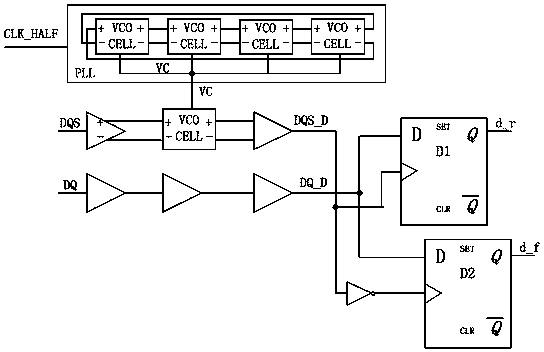
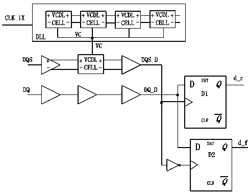
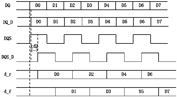
[0030] For a DDR memory connected to the SOC chip, according to the timing requirements of the read and write operations of the DDR memory, when the read operation is performed, the data pulse selection signal DQS and the data signal DQ need to be edge-aligned. The embodiment of the present invention provides a kind of read data signal processing circuit of DDR memory, such as Figure 4 with Figure 5 As shown, the sampling receiving module for receiving the data pulse selection signal DQS and the data signal DQ of the DDR memory outside the SOC chip and the pulse width for generating the digital control signal TD[n-1:0] with controllable delay Test module; wherein, the pulse width test module is used to output a high-level pulse signal CK_PULSE according to the clock signal CLK_X provided in the SOC chip, wherein the frequency of the clock signa...
PUM
 Abstract
Description
Claims
Application Information