

A Method for On-Line Monitoring of the Shape of the Crystal Growth Interface in a Czochralski Single Crystal Furnace
A single crystal furnace and crystal growth technology, which is applied in the field of Czochralski single crystal growth, can solve the problem of difficult observation of the shape of the growth crystal interface
- Summary
- Abstract
- Description
- Claims
- Application Information
AI Technical Summary
Problems solved by technology
Method used
Image

Examples
Embodiment Construction
[0018] The present invention will be described in further detail below in conjunction with the accompanying drawings.
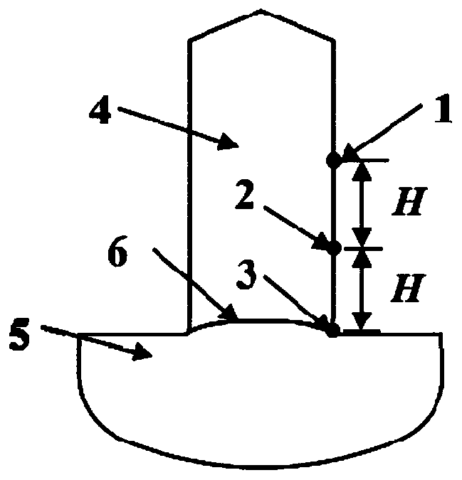
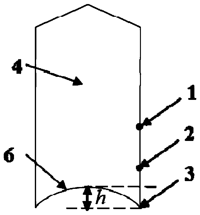
[0019] like figure 1 As shown, the present invention provides a method for on-line monitoring the shape of the crystal growth interface in a Czochralski single crystal furnace. The method includes: arranging two temperature monitoring points on the side wall of the high-temperature crystal 4, respectively the first temperature monitoring point 1 and the first temperature monitoring point 1. Second temperature monitoring point 2. In particular, the distance H between the first temperature monitoring point 1 and the second temperature monitoring point 2 and the triple point 3 is equal to 2-20 cm. During the entire crystal pulling process, the positions of the first temperature monitoring point 1 and the second temperature monitoring point 2 remain unchanged. The shape of the growth interface is generally described by the convexity h of the growth interface, s...
PUM
 Abstract
Description
Claims
Application Information