Backlight illumination hybrid chip antireflection film growth method and device

An anti-reflection film and chip technology, which is applied in the field of infrared detectors, can solve problems such as chip performance degradation, chip temperature rise, and failure, and achieve the effects of reducing growth temperature, reducing temperature accumulation, and preventing coating

Inactive Publication Date: 2018-12-07
11TH RES INST OF CHINA ELECTRONICS TECH GROUP CORP
View PDF5 Cites 0 Cited by
  • Summary
  • Abstract
  • Description
  • Claims
  • Application Information

AI Technical Summary

Problems solved by technology

[0005] The present invention provides a method and device for growing an anti-reflection film on a back-illuminated hybrid chip to solve the problem in the prior

Method used


Image

  • Backlight illumination hybrid chip antireflection film growth method and device
  • Backlight illumination hybrid chip antireflection film growth method and device
  • Backlight illumination hybrid chip antireflection film growth method and device

Examples


Embodiment Construction

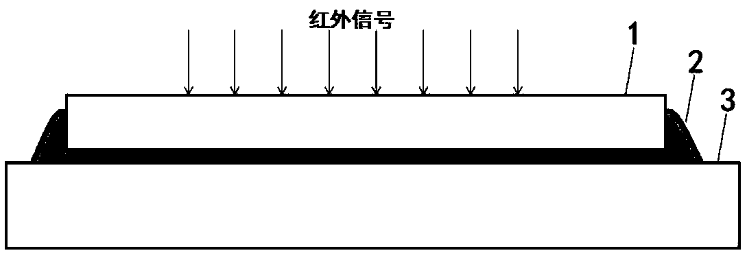
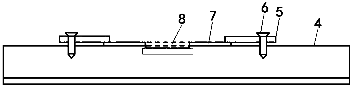
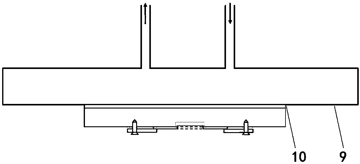
[0028] In order to solve the problem of chip temperature rise caused by the growth process of the back anti-reflection film layer in the prior art, resulting in chip performance degradation or even failure, the present invention provides a backlight hybrid chip anti-reflection film growth method and device. The infrared focal plane hybrid chip 8 is packaged in the sample tray, and a thermal pad is arranged on the back of the sample tray 4, thereby improving the heat conduction efficiency between the sample tray 4 and the cooling workpiece tray 9, and reducing the growth of the anti-reflection film layer on the back of the hybrid chip through rapid heat conduction The temperature accumulation during the time reduces the growth temperature and avoids performance degradation or even failure of the hybrid chip due to excessive temperature. Moreover, the present invention can form an effective shield when the back anti-reflection film layer grows by adopting the design of the shieldi...


PUM


Abstract

The invention discloses a backlight illumination hybrid chip antireflection film growth method and device. An infrared focal plane hybrid chip is packaged in a sample tray, a heat conduction pad is placed on the back of the sample tray, so heat conduction efficiency of the sample tray and a cooling workpiece tray is improved, temperature accumulation during growth of a back antireflection film layer of the hybrid chip is reduced through rapid temperature conduction, the growth temperature is reduced, performance degradation or even failure of the hybrid chip caused by the excessive temperaturecan be avoided, through designing a shielding film, effective blocking can be formed when the back antireflection film layer grows, and the surface of glue and a readout circuit is prevented from being coated while the chip is being coated.

Description

technical field [0001] The invention relates to the technical field of infrared detectors, in particular to a method and device for growing an antireflection film on a backlight hybrid chip. Background technique [0002] Infrared detector components, especially mercury cadmium telluride infrared focal plane detector components, have promoted the development of infrared technology applications and greatly improved the performance of infrared weapons and equipment. They have been used in military systems such as reconnaissance, surveillance, precision guidance, search and tracking, and photoelectric countermeasures. , has become an important part of advanced optoelectronic weapon systems, and is also widely used in civilian fields such as driver assistance, fire protection, security, and production safety. [0003] The mercury cadmium telluride infrared focal plane hybrid chip is the core component of the infrared detector assembly and is used for infrared radiation signal con...

Claims


Application Information

Patent Timeline
IPC IPC(8): H01L27/146
CPCH01L27/14685
Inventor 宁提吴立明祁娇娇王玉龙
Owner 11TH RES INST OF CHINA ELECTRONICS TECH GROUP CORP
Why Eureka
Try Eureka