LED linear constant current drive circuit with adaptive wide voltage range
A linear constant current drive and wide voltage technology, applied in the field of integrated circuits, can solve the problems of insufficient utilization and waste of LEDs, and achieve the effect of long life and good stability
- Summary
- Abstract
- Description
- Claims
- Application Information
AI Technical Summary
Problems solved by technology
Method used
Image

Examples
Embodiment Construction
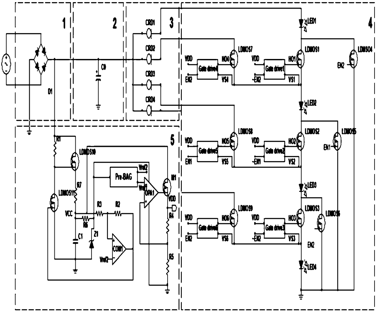
[0023] Rectifier bridge 1, for full-wave rectification of the 85V-265V / 50Hz sinusoidal voltage waveform; it is a full-wave rectifier bridge, connected with the filter circuit and the high-voltage voltage regulator and step-down circuit through wires;
[0024] The filter circuit 2 is used to filter out high-frequency components in the rectified pulsating voltage; the filter circuit is composed of electrolytic capacitors to realize filtering.
[0025] The constant current source circuit 3 is used to limit the current flowing through the load LED light string, and provide constant current power for the LED light. The constant current source circuit has four branches, and each constant current branch includes a two-terminal constant current device CRD. The CRD has a wide range of constant current voltage. Since the LED itself has a certain voltage clamping function, when the input AC voltage changes within a wide range, the fluctuation of the output voltage of the rectifier bridge...
PUM
 Abstract
Description
Claims
Application Information