PCB secondary and multiple accurate punching method based on visual tracking

A PCB board and visual tracking technology, which is applied in the direction of circuit board tool positioning, electrical components, printed circuit manufacturing, etc., can solve the problems of insufficient precision of PCB board punching technology, unsuitable printed plugs, etc., to facilitate extraction and Positioning, image background interference is less, and the effect of ensuring accuracy

Inactive Publication Date: 2018-12-07
向耀
View PDF7 Cites 10 Cited by
  • Summary
  • Abstract
  • Description
  • Claims
  • Application Information

AI Technical Summary

Problems solved by technology

[0003] In the stage of PCB board design, designers usually make Mark points as positioning benchmarks. Only with accurate positional relationship can it be used for subsequent effective position detection; the patent document with application number: 201510795283.8 discloses a PCB based on machine vision. Solder joint positioning method; directly use the position of the identified Mark point to realize butt welding; however, the accuracy of this direct identification of the position of the Mark point is not enough in the PCB board drilling technology, and it is easy to cause subsequent use. Cases where the position does not match the printed plug

Method used


Image

  • PCB secondary and multiple accurate punching method based on visual tracking
  • PCB secondary and multiple accurate punching method based on visual tracking
  • PCB secondary and multiple accurate punching method based on visual tracking

Examples


Embodiment Construction

[0026] In order to express the present invention more clearly, the present invention will be further described below in conjunction with the accompanying drawings.

[0027] For some English abbreviations covered in the present invention, the next paragraph focuses on the meaning of these English abbreviations.

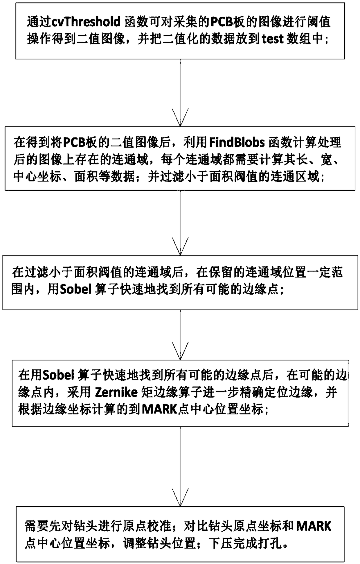
[0028] For example: the Mark point of the PCB board is the position recognition point of the PCB board applied to the automatic placement machine in the circuit board design, also called a mark point or a feature point; it is the overall shape of an image target, described by a high-order moment feature vector is the detail of the image target.

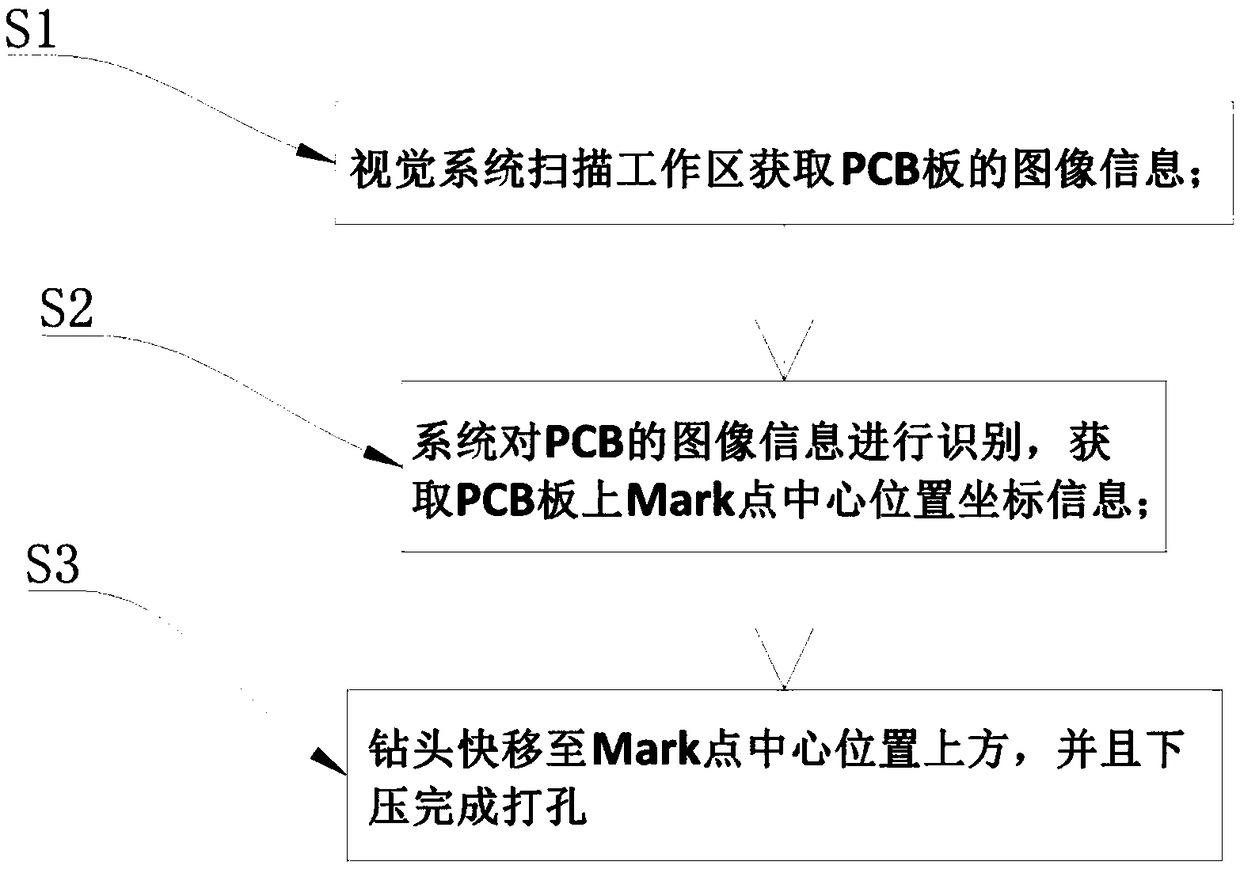
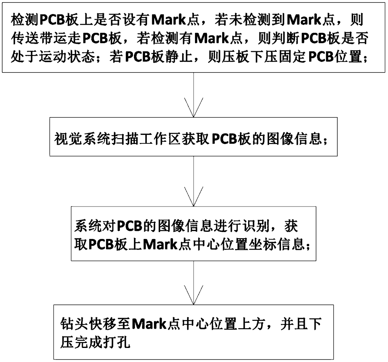
[0029] see figure 1 , the present invention takes the processing process as an example, and specifically illustrates the PCB board punching method utilizing Mark point positioning, specifically comprising the following steps:

[0030] S1: Put the PCB board to be tested on the acquisition surface of the vision system, select ...


PUM


Abstract

The invention discloses a PCB secondary and multiple accurate punching method based on visual tracking. After the image information of the PCB is obtained through the vision system, the image information is subjected to binaryzation through a cvThreshold function; calculating a communication domain which exists on the processed image by utilizing a FindBlobs function, and filtering the communication domain which is smaller than the area; accurately positioning the edge by means of a Zernike moment edge operator in the possible edge points after all possible edge points are quickly found through a Sobel operator, and calculating to obtain the center position coordinates of the Mark points or the prefabricated hole according to the edge coordinates. The data volume of the points needing to be calculated is greatly reduced, and the speed of determining the center coordinates is increased, and the accuracy is not lost; by adopting a multi-time punching mode, the center coordinates of the prefabricated hole are positioned again during each punching, and the deviation problem possibly caused by single positioning is corrected, the drill bit is a grinding process of the edge of the prefabricated hole punched previously during multiple times of punching, and the precision is far higher than that of the single punching.

Description

technical field [0001] The invention relates to the field of PCB drilling, in particular to a method for secondary and multiple accurate drilling of PCB boards based on vision tracking. Background technique [0002] With the development of computer digital image processing technology and non-destructive testing technology, detection and recognition technology is increasingly developing towards intelligent, high-reliability, high-speed automatic online detection; computer vision technology and reliability technology are the two major technologies of modern detection Basic; machine vision has been successfully applied in the field of industrial inspection, which includes automatic inspection of PCB boards (ie: printed circuit boards), automatic positioning of circuit boards and calibration of benchmarks, and accurate inspection of Obtaining the location of components plays an important role. [0003] In the stage of PCB board design, designers usually make Mark points as posi...

Claims


Application Information

Patent Timeline
Patent Type & Authority Applications(China)
IPC IPC(8): H05K3/00
CPCH05K3/0008H05K3/0047H05K2203/1476
Inventor 向耀
Owner 向耀
Why Eureka
Try Eureka