Liquid crystal display and its substrate structure

A liquid crystal display and substrate technology, applied in instruments, optics, nonlinear optics, etc., can solve problems such as uneven diffusion of PI liquid, and achieve the effect of avoiding uneven diffusion of PI liquid and improving product yield and competitiveness.

Active Publication Date: 2021-10-29
TCL CHINA STAR OPTOELECTRONICS TECH CO LTD
View PDF4 Cites 0 Cited by
  • Summary
  • Abstract
  • Description
  • Claims
  • Application Information

AI Technical Summary

Problems solved by technology

[0003] In order to solve the above problems, the present invention provides a liquid crystal display and its substrate structure, which can solve the phenomenon of uneven diffusion of PI liquid at the edge of the display area, and improve product yield and competitiveness

Method used


Image

  • Liquid crystal display and its substrate structure
  • Liquid crystal display and its substrate structure
  • Liquid crystal display and its substrate structure

Examples


Embodiment 1

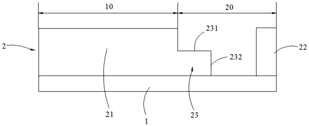
[0027] refer to figure 1 , figure 2 , the liquid crystal display of this embodiment has a display area 10 and a non-display area 20, and the non-display area 20 corresponds to the frame of the liquid crystal display. A liquid crystal display CF substrate, wherein the CF substrate includes a black matrix layer 1 and a color-resist layer 2, the color-resist layer 2 is arranged on the black matrix layer 1, and the color-resist layer 2 includes a first color-resist structure 21 and a second color-resist structure 22 , the second color-resisting structure 22 is disposed around the first color-resisting structure 21 and is spaced apart from the first color-resisting structure 21 . The color-resist layer 2 further includes a first step portion 23 protruding from the sidewall of the first color-resist structure 21 , and the first step portion 23 includes a portion extending from the sidewall of the first color-resist structure 21 toward the second color-resist structure 22 . The fi...

Embodiment 2

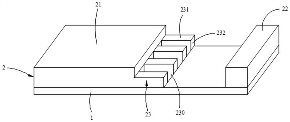
[0034] refer to image 3 , Figure 4 The difference between the CF substrate in this embodiment and the CF substrate in Embodiment 1 is that the number of first stepped portions 23 is at least two. The distances from the first stepped surfaces 231 of the at least two first stepped portions 23 to the black matrix layer 1 gradually decrease along the direction approaching the second color resist structure 22 .

[0035] At least two first stepped portions 23 correspond to the non-display area 20 of the liquid crystal display. In the alignment film printing process, the PI liquid dripped on the surface of the first color-resist structure 21 spreads to both sides, flows from the edge of the first color-resist structure 21 sequentially through at least two first steps 23, and then accumulates to the first color-resist structure. Between the resistance structure 21 and the second color resistance structure 22, when the PI liquid flows down from the edge of the first color resistanc...

Embodiment 3

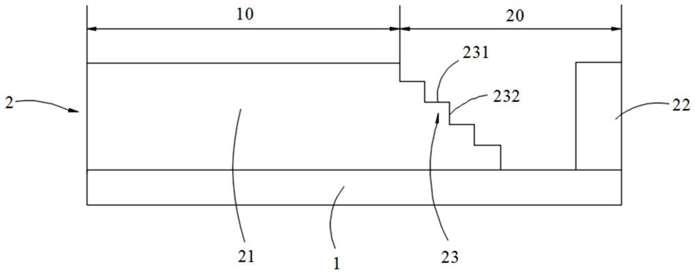
[0040] refer to Figure 5 , Figure 6 The difference between the CF substrate in this embodiment and the CF substrate in Embodiment 2 is that the color-resist layer 2 further includes at least one second step portion 24 protruding inside the second color-resist structure 22, and the second step The portion 24 includes a third stepped surface 241 extending from the inner side of the second color-resisting structure 22 toward the first color-resisting structure 21 and a fourth stepped surface 242 extending from the third stepped surface 241 toward the black matrix layer 1, at least one The distance from the third stepped surface 241 of the second stepped portion 24 to the black matrix layer 1 gradually decreases along the direction approaching the first color resist structure 21 .

[0041] A plurality of second grooves 240 are arranged at intervals on the third step surface 241 of at least one second step portion 24 , and opening directions of the plurality of second grooves 24...


PUM


Abstract

The present invention provides a liquid crystal display and its substrate structure. The substrate structure includes a substrate and a color-resist layer. The color-resist layer includes a first color-resist structure and a second color-resist structure. The second color-resist structure is arranged around the first color-resist structure and Set apart from the first color-resisting structure, the color-resisting layer further includes at least one first step portion protruding from the sidewall of the first color-resisting structure, the first step portion includes The first stepped surface extended from the structure and the second stepped surface substantially extended from the first stepped surface, the distance from the first stepped surface of at least one first stepped portion to the substrate is along the direction close to the second color resist structure In descending order, the PI liquid on the first color-resisting structure is guided to between the first color-resisting structure and the second color-resisting structure through at least one first step, reducing the backflow of the PI liquid when it is blocked by the second color-resisting structure Speed, so as to avoid the phenomenon that the PI liquid is backflowed and accumulated on the surface of the first color-resisting structure, which causes uneven diffusion of the PI liquid at the edge of the display area.

Description

technical field [0001] The invention relates to the technical field of preparation technology of liquid crystal displays, in particular to a liquid crystal display and its substrate structure. Background technique [0002] The alignment film printing process is a very important production process in the production process of liquid crystal displays. The alignment film layer is used on liquid crystal displays because of its unique insulating properties and alignment characteristics. At present, the alignment film printing process is generally divided into There are two types, one is the roller coating method. The advantage of this method is that it can better control the diffusivity of the alignment liquid, that is, the PI (Polyimide, polyimide) liquid, and the thickness uniformity and Coating accuracy is relatively easy to control, but when making large-size panels, the uniformity of the thickness of the patterned film layer after coating cannot be well managed due to the la...

Claims


Application Information

Patent Timeline
Patent Type & Authority Patents(China)
IPC IPC(8): G02F1/1333G02F1/1337
CPCG02F1/1333G02F1/133723
Inventor 谢克成
Owner TCL CHINA STAR OPTOELECTRONICS TECH CO LTD
Why Eureka
Try Eureka