A preparation method of a shielded gate power device

A technology for power devices and shielded gates, which is applied in the manufacture of semiconductor/solid-state devices, semiconductor devices, electrical components, etc., can solve the problems of large static power loss, large switching power loss of shielded gate power MOSFETs, and large on-state resistance, etc. The effect of improving reverse withstand voltage, small on-state resistance and reducing capacitance

Inactive Publication Date: 2018-12-18
厦门芯一代集成电路有限公司
View PDF3 Cites 5 Cited by
  • Summary
  • Abstract
  • Description
  • Claims
  • Application Information

AI Technical Summary

Problems solved by technology

[0003] The existing structure mostly adopts single-layer uniform resistivity epitaxy, because of its large on-state resistance and large static power loss; the shielded gate is uniform N-type doped polysilicon, and the capacitance between the shielded gate and the drain is relatively large. The switching power loss of the power MOSFET is large

Method used


Image

  • A preparation method of a shielded gate power device
  • A preparation method of a shielded gate power device
  • A preparation method of a shielded gate power device

Examples


Embodiment Construction

[0025] Specific embodiments of the present invention will be described in detail below in conjunction with the accompanying drawings.

[0026] As shown in the figure, a method for manufacturing a shielded gate power device includes the following steps:

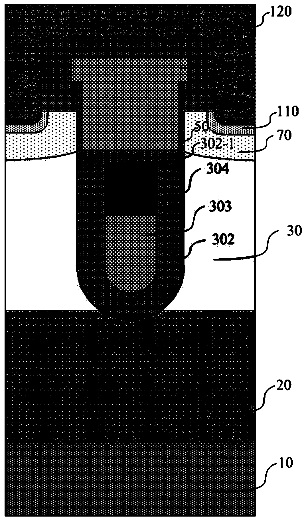
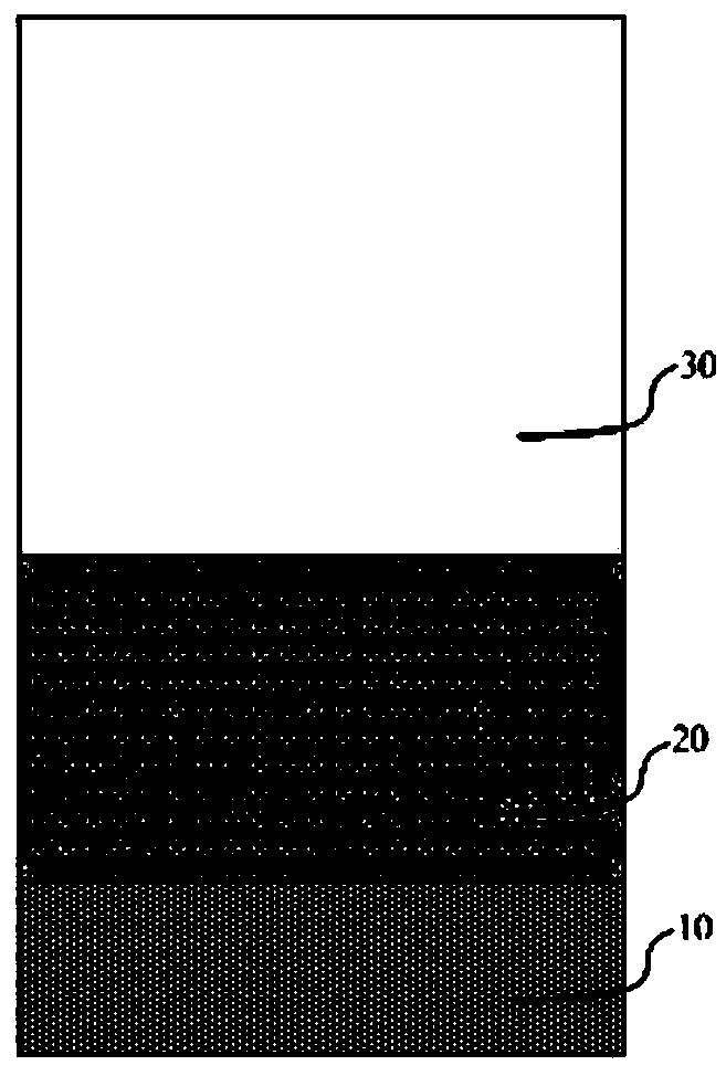
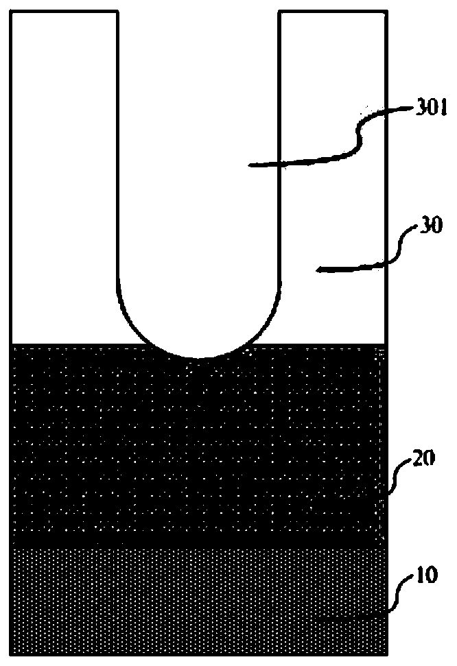
[0027] Step 1. Provide an N-type heavily doped semiconductor substrate (10), grow a first epitaxial layer and a second epitaxial layer on the N-type heavily doped semiconductor substrate (10), and the first epitaxial layer is The low resistance layer (20), and the second epitaxial layer is a high resistance layer (30). The gate oxide extends vertically toward the drain, and the Resurf technology is used to optimize the lateral electric field distribution of the upper high-resistance layer (30) to improve the reverse withstand voltage of the device, and the lower layer is epitaxy to reduce the device’s On-state resistance;

[0028] Step 2, etching the high-resistance layer (30) to form a trench (301), the bottom of the trench...


PUM


Abstract

An object of the present invention is to provide a preparation method of a shielded gate power device. A double-layer different resistivity epitaxy is adopted, the lower layer is low resistance epitaxy, which has smaller on-state resistance than the homogeneous high resistance epitaxial layer under the same withstand voltage to reduce the static power loss of the device, the gate oxide longitudinally extends to the drain, and the transverse electric field distribution of the upper layer high resistance layer is optimized by a Resurf technology, so as to improve the reverse withstand voltage ofthe device. As the shield gate is PN-doped polysilicon, the capacitance between the shield gate and the drain can be reduced so as to reduce the switch power loss of the shielded gate power MOSFET.

Description

technical field [0001] The invention relates to a method for preparing a power device, in particular to a method for preparing a shielded grid power device. Background technique [0002] Since the invention of power MOS technology, there have been many important developments and advancements in the technology. In recent years, new device structures and new manufacturing processes of power MOS technology have emerged continuously to achieve two basic goals: maximum power handling capability and minimum power loss. [0003] The existing structure mostly adopts single-layer uniform resistivity epitaxy, because of its large on-state resistance and large static power loss; the shielded gate is uniform N-type doped polysilicon, and the capacitance between the shielded gate and the drain is relatively large. The switching power loss of the power MOSFET is relatively large. Contents of the invention [0004] In order to solve the above problems, the object of the present inventi...

Claims


Application Information

Patent Timeline
Patent Type & Authority Applications(China)
IPC IPC(8): H01L21/336H01L29/78H01L29/06
CPCH01L29/063H01L29/0634H01L29/66621H01L29/66666H01L29/7827H01L29/66734H01L29/7813H01L29/407
Inventor 张军亮陈利陈译
Owner 厦门芯一代集成电路有限公司
Why Eureka
Try Eureka