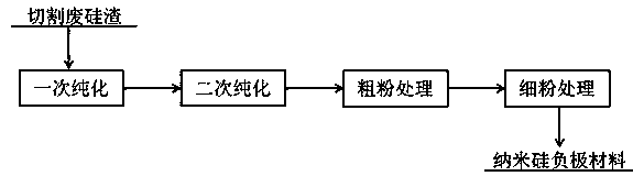
A method for preparing nano-silicon anode materials by using waste silicon slag from the photovoltaic industry
A negative electrode material and nano-silicon technology, which is applied in battery electrodes, structural parts, electrical components, etc., can solve the problems of high energy consumption, harsh environmental requirements, and low production efficiency of the plasma method, and achieve a widened production and sales chain and low cost. , the effect of increasing added value
- Summary
- Abstract
- Description
- Claims
- Application Information
AI Technical Summary
Problems solved by technology
Method used
Image

Examples
Embodiment 1
[0032] The method for preparing nano-silicon anode material by utilizing waste silicon slag in the photovoltaic industry in this embodiment, the steps are as follows:
[0033] (1) Put the cutting waste silicon slag into the block crusher to obtain waste silicon with a particle size of less than 2 mm. Subsequently, 5 kg of crushed silicon waste was slowly immersed in 20 L of 1 M dilute hydrochloric acid at a stirring speed of 200 rpm at 50 °C for 70 min. Filter, then wash with deionized water until neutral, and dry in a vacuum drying oven at 120 °C until the moisture is less than 2%, to obtain waste silicon powder after primary purification;
[0034] (2) Put the waste silicon powder after primary purification into the block grinder, and crush the dried silicon powder to less than 2 mm. Then, put it into a horizontal tube furnace, first pass through Ar to purge for 10 min, then raise the temperature from room temperature to 700 °C at a rate of 5 °C / min, and keep it for 2 h to o...
Embodiment 2
[0041] The method for preparing nano-silicon anode material by utilizing waste silicon slag in the photovoltaic industry in this embodiment, the steps are as follows:
[0042] (1) Put the cutting waste silicon slag into the block crusher to obtain waste silicon with a particle size of less than 2 mm. Subsequently, 5 kg of crushed silicon waste was slowly immersed in 20 L of 1 M dilute sulfuric acid at a stirring speed of 200 rpm at 50 °C for 60 min. Filter, then wash with deionized water until neutral, and dry in a vacuum drying oven at 110 °C until the moisture is less than 2%, to obtain waste silicon powder after primary purification;
[0043] (2) Put the waste silicon powder after primary purification into the block grinder, and crush the dried silicon powder to less than 2 mm. Then, it was put into a horizontal tube furnace, first passed through Ar to purge for 10 min, then raised from room temperature to 700 °C at a rate of 5 °C / min, and kept for 2 h to obtain the second...
Embodiment 3
[0048] The method for preparing nano-silicon anode material by utilizing waste silicon slag in the photovoltaic industry in this embodiment, the steps are as follows:
[0049] (1) Put the cutting waste silicon slag into the block crusher to obtain waste silicon with a particle size of less than 2 mm. Subsequently, 5 kg of crushed silicon waste was slowly immersed in 20 L of 1 M dilute nitric acid at a stirring speed of 200 rpm at 50 °C for 50 min. Filter, then wash with deionized water until neutral, and dry in a vacuum oven at 100 °C until the moisture is less than 2%, to obtain a purified waste silicon powder;
[0050] (2) Put the waste silicon powder after primary purification into the block grinder, and crush the dried silicon powder to less than 2 mm. Then, it was put into a horizontal tube furnace, first passed through Ar to purge for 10 min, then raised from room temperature to 700 °C at a rate of 5 °C / min, and kept for 2 h to obtain the secondary purified silicon pin...
PUM
| Property | Measurement | Unit |
|---|---|---|
| particle size | aaaaa | aaaaa |
| particle diameter | aaaaa | aaaaa |
| purity | aaaaa | aaaaa |
Abstract
Description
Claims
Application Information