
A programming method and a device of a nonvolatile memory

A technology of non-volatile and programming methods, which is applied in the field of non-volatile memory programming methods and devices, and can solve the problems of low logic circuit utilization and large circuit area

Active Publication Date: 2018-12-25
GIGADEVICE SEMICON (BEIJING) INC
View PDF5 Cites 3 Cited by
  • Summary
  • Abstract
  • Description
  • Claims
  • Application Information

AI Technical Summary

Problems solved by technology

[0004] When the inventor applied the prior art, he found that the SRAM in the prior art was only used to store the data to be programmed, and the verification result after verifying the data to be programmed and the data information in the non-volatile memory was updated to In the storage device A, the SRAM is in an idle state, resulting in a low utilization rate of the logic circuit, and because an additional storage device is provided, the area of ​​the circuit is relatively large

Method used


Image

  • A programming method and a device of a nonvolatile memory
  • A programming method and a device of a nonvolatile memory
  • A programming method and a device of a nonvolatile memory

Examples


Embodiment 1

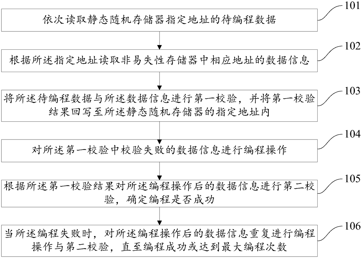
[0063] refer to figure 1 , which shows a flow chart of a non-volatile memory programming method in Embodiment 1 of the present invention, which may specifically include the following steps:

[0064] Step 101 , sequentially read the data to be programmed at the designated address of the SRAM.

[0065] In the embodiment of the present invention, the data to be programmed at the specified address of the SRAM is sequentially read in order. For the data to be programmed in a page in the SRAM, the data to be programmed is read sequentially from the first address of the page until the page is read. tail address.

[0066] Wherein, a page can also be described as 1 page, and the data of 1 page is 256 bytes (bytes), and the static random access memory can also be described as SRAM (Static Random Access Memory, static random access memory).

[0067] For example, the data to be programmed is stored in the range of 0-255 in a certain row of the SRAM, and the data to be programmed is sequ...

Embodiment 2

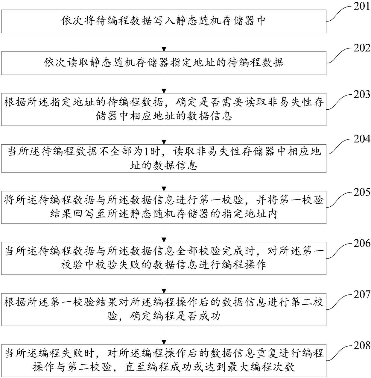
[0087] refer to figure 2 , which shows a flow chart of a non-volatile memory programming method in Embodiment 2 of the present invention, which may specifically include the following steps:

[0088] Step 201, sequentially write the data to be programmed into the SRAM.

[0089] In the embodiment of the present invention, the data to be programmed is sequentially written into the SRAM.

[0090] In step 202, the data to be programmed at the specified address of the SRAM is sequentially read.

[0091] This step is the same as step 101 in Embodiment 1, and will not be described in detail here.

[0092] Step 203, according to the data to be programmed at the specified address, determine whether it is necessary to read the data information of the corresponding address in the non-volatile memory.

[0093] In the embodiment of the present invention, according to the read data to be programmed at the specified address of the SRAM, it is determined whether it is necessary to read the...

Embodiment 3

[0117] refer to Figure 4 , shows a structural block diagram of a non-volatile memory programming device in Embodiment 3 of the present invention.

[0118] The programming device 400 of the non-volatile memory of the embodiment of the present invention includes:

[0119] The data to be programmed reading module 401 is used for sequentially reading the data to be programmed at the specified address of the SRAM.

[0120] The data information reading module 402 is configured to read the data information of the corresponding address in the non-volatile memory according to the specified address.

[0121] The first verification module 403 is configured to perform a first verification on the data to be programmed and the data information, and write back the first verification result to a specified address of the SRAM.

[0122] A programming operation module 404, configured to perform a programming operation on data information that fails verification in the first verification.

[...


PUM


Abstract

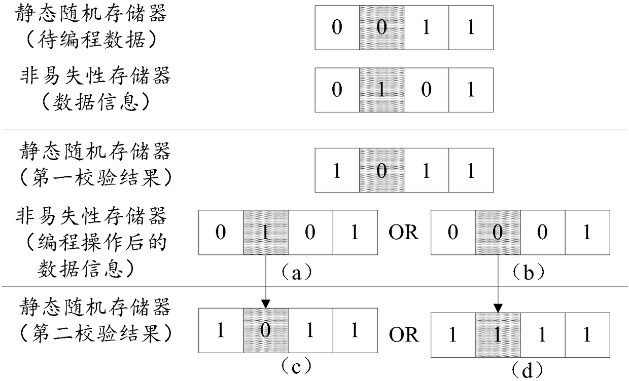
The embodiment of the invention provides a programming method and a device of a nonvolatile memory, which relate to the technical field of memory. The embodiment of the invention performs a first check on the data to be programmed in the static random access memory and the data information in the non-volatile memory, the first check result is written back into the static random access memory, thedata information failed in the first check is programmed, and the second check is performed on the data information after the programming operation according to the first check result to determine whether the programming is successful or not. By writing back the check result to SRAM, and judging whether to program the data information in the nonvolatile memory according to the checking result in the static random access memory, by using the idea of time-sharing multiplexing, the SRAM can not only store the data to be programmed, but also store the verification result instead of the memory device A. The utility rate of the logic circuit is improved, the logic structure is simplified, and the area of the circuit is reduced.

Description

technical field [0001] The invention relates to the technical field of memory, in particular to a programming method and device for a nonvolatile memory. Background technique [0002] Non-volatile memory is a kind of memory that can maintain the stored data in the case of power failure. Therefore, non-volatile memory is widely used as data storage for electronic products such as computers, personal digital assistants, mobile phones, and digital cameras. storage device. [0003] At present, the programming method of the non-volatile memory is to write the data to be programmed in one page into the SRAM, verify the data to be programmed with the original data information in the non-volatile memory, and store the verification result in In an additional storage device A, it is judged according to the verification result in the storage device A whether to program the original data information in the non-volatile memory. [0004] When the inventor applied the prior art, he found...

Claims


Application Information

Patent Timeline
IPC IPC(8): G11C16/10G11C16/34
CPCG11C16/10G11C16/3454
Inventor 杨莹
Owner GIGADEVICE SEMICON (BEIJING) INC
Learn More