Driving circuit of electric power conversion unit, driving method, electric power conversion unit, and electric power conversion device
A power conversion device and power conversion technology, applied in the direction of output power conversion devices, electrical components, etc., can solve the problems of large-capacity and cost-effective power conversion devices, and achieve the effect of reducing accuracy or reliability
- Summary
- Abstract
- Description
- Claims
- Application Information
AI Technical Summary
Problems solved by technology
Method used
Image

Examples
Embodiment 1
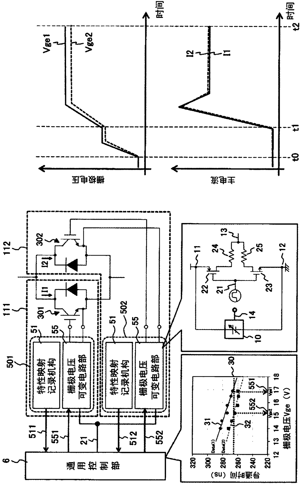
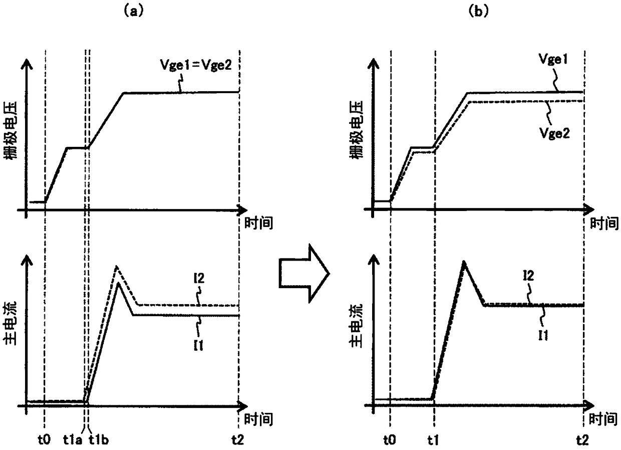
[0034] figure 1 A block diagram showing a drive circuit of the power conversion unit according to Embodiment 1 of the present invention. In addition, an example of a gate voltage waveform and an example of a main current waveform are described together.
[0035] The current conversion device is composed of a power conversion unit 111 and a power conversion unit 112 . The power conversion unit 111 and the power conversion unit 112 are connected in parallel to each other, and are controlled by the common control unit 6 . In addition, the number of power conversion units connected in parallel is not limited to two, and may be multiple according to the power capacity of the power conversion device.
[0036] The power conversion unit 111 is composed of a power semiconductor switching element 301 and a drive circuit 501 . The power conversion unit 112 is composed of a power semiconductor switching element 302 and a drive circuit 502 . The semiconductor switching element 301 and ...
Embodiment 2
[0072] Figure 5 A block diagram showing a driving circuit of a power conversion unit according to Embodiment 2 of the present invention. Hereinafter, the points different from the first embodiment will be mainly described.
[0073] In Embodiment 2, the characteristic map information 31, 32 ( figure 1 ) is obtained by reference from the database 201.
[0074] like Figure 5 As shown, characteristic map information representing the relationship between the switching characteristic of each semiconductor switching element and the gate driving voltage is stored in the database 201 . The power conversion unit 111 and the power conversion unit 112 are associated with the characteristic mapping information in the database 201 by using identification mechanisms such as product barcodes or manufacturing numbers attached to them.
[0075] When the power conversion unit 111 and the power conversion unit 112 are connected in parallel, the computer 203 uses the reading mechanism 202 to...
Embodiment 3
[0080] Image 6 A block diagram showing a drive circuit of a power conversion unit according to Embodiment 3 of the present invention. Hereinafter, the points different from the first embodiment will be mainly described.
[0081] The power conversion unit 111 is composed of a power module 305 including upper and lower arms, a driving circuit 503 for driving the semiconductor switching element 303 of the upper arm, and a driving circuit 501 for driving the semiconductor switching element 301 of the lower arm. Furthermore, the power conversion unit 112 is composed of a power module 306 including upper and lower arms, a driving circuit 504 for driving the semiconductor switching element 304 of the upper arm, and a driving circuit 502 for driving the semiconductor switching element 302 of the lower arm.
[0082] The power conversion unit 111 and the power conversion unit 112 are connected in parallel to constitute one phase of a main circuit of a power conversion device (for exam...
PUM
 Abstract
Description
Claims
Application Information
 - R&D Engineer
- R&D Manager
- IP Professional
- Industry Leading Data Capabilities
- Powerful AI technology
- Patent DNA Extraction
Browse by: Latest US Patents, China's latest patents, Technical Efficacy Thesaurus, Application Domain, Technology Topic.
© 2024 PatSnap. All rights reserved.Legal|Privacy policy|Modern Slavery Act Transparency Statement|Sitemap