Organic electroluminescent display panel, manufacturing method and display device thereof

A technology of electroluminescent display and display panel, which is applied in the direction of circuits, electrical components, static indicators, etc., and can solve the problems of display panels such as difficulty in setting narrow borders

Pending Publication Date: 2019-01-11
BOE TECH GRP CO LTD +1
View PDF9 Cites 8 Cited by
  • Summary
  • Abstract
  • Description
  • Claims
  • Application Information

AI Technical Summary

Problems solved by technology

[0004] In view of this, the embodiments of the present invention provide an organic electroluminescence display panel, a manufacturing method thereof, and a display device, so as to solve the problem that it is difficult to realize a narrow frame setting in an existing display panel.

Method used


Image

  • Organic electroluminescent display panel, manufacturing method and display device thereof
  • Organic electroluminescent display panel, manufacturing method and display device thereof
  • Organic electroluminescent display panel, manufacturing method and display device thereof

Examples


Embodiment Construction

[0025] The specific implementation manners of the organic electroluminescent display panel provided by the embodiments of the present invention, its manufacturing method and the display device will be described in detail below with reference to the accompanying drawings.

[0026] The thickness and area shape of each film layer in the drawings do not reflect the true proportion of the organic electroluminescent display panel, but are only intended to schematically illustrate the content of the present invention.

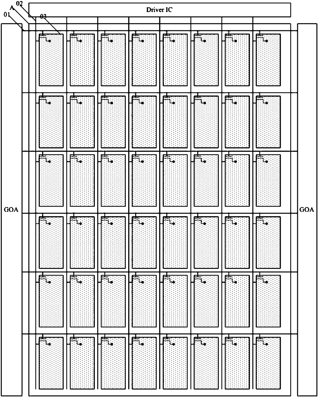
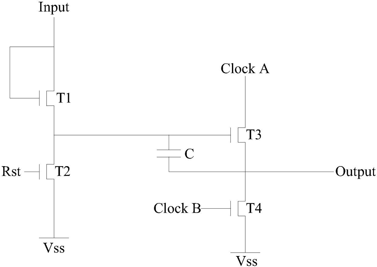
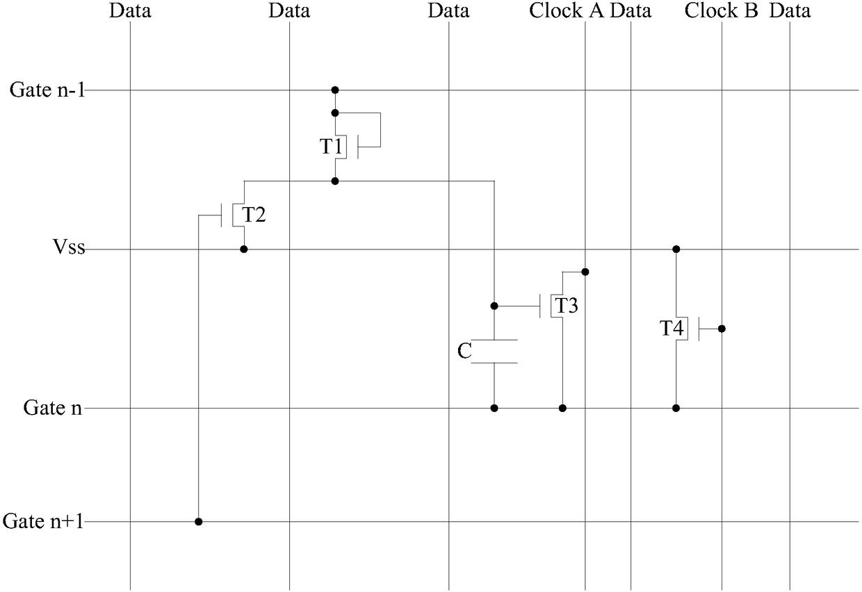
[0027] An embodiment of the present invention provides an organic electroluminescent display panel, such as Figure 4 to Figure 6 As shown, it includes: a base substrate 100, a plurality of pixel drive circuits 200 and a gate drive circuit 300 arranged in the display area A of the base substrate 100, and a covering pixel drive circuit 200 and a gate drive circuit 200 arranged in the display area A of the base substrate 100. A plurality of top emission light emitting u...


PUM


Abstract

An organic electroluminescent display panel, a manufacturing method and display device thereof are disclosed. A gate drive circuit and a pixel driving circuit are simultaneously arranged in a displayarea of a substrate base plate, and that regions where the gate driving circuit and the pixel drive circuit are located are not overlapped with each other. A plurality of top emission type light emitting units covering a pixel driving circuit and a gate driving circuit are provided in a display region of a substrate, That is to say, the occupied area of each top-emitting light-emitting unit is increased, from the existing top-emitting light-emitting unit overlapping only one pixel driving circuit to an overlapping area between the gate driving circuit and the top-emitting light-emitting unit in the display area, so as to ensure that all the circuits in the display area are covered by the top-emitting light-emitting unit. This can ensure that the gate driving circuit and pixel driving circuit have enough wiring space in the display region, save the wiring space of the gate driving circuit at the border, and realize the ultra-narrow border or even border-free design.

Description

technical field [0001] The present invention relates to the field of display technology, in particular to an organic electroluminescence display panel, a manufacturing method thereof and a display device. Background technique [0002] Currently, if figure 1 As shown, the display area A in the display panel is provided with gate lines 01, data lines 02, and pixel units 03 arranged in the area defined by the gate lines 01 and data lines 02, and the left and right borders are provided for driving the gate lines. 01 gate drive circuit GOA. Specifically, the gate drive circuit GOA is composed of multiple cascaded shift registers, and the circuit structure diagram of each shift register is as follows figure 2 As shown, it is composed of at least four switching transistors T1, T2, T3 and T4. [0003] At present, the requirements for the bezel of display products in the market are getting higher and higher, and ultra-narrow bezel or even bezel-less design is expected, but the ab...

Claims


Application Information

Patent Timeline
Patent Type & Authority Applications(China)
IPC IPC(8): H01L27/32H01L27/02
CPCH01L27/0207G09G3/3225G09G2310/0264H01L27/02G09G2300/0426G09G2300/0408G09G3/3266G09G2310/0286H10K59/00H10K59/121H10K59/1213H10K59/131G09G2310/0281H10K59/1201
Inventor 高永益谭文黄炜赟王本莲
Owner BOE TECH GRP CO LTD
Why Eureka
Try Eureka