
Assembly for mounting driver IC

A driver and component technology, applied in the manufacture of electric solid-state devices, semiconductor devices, semiconductor/solid-state devices, etc., can solve the problems of drive wiring system width and area limitations, and achieve the effects of stable control operation, noise suppression, and line impedance suppression

Inactive Publication Date: 2005-08-10
FUJITSU LTD
View PDF4 Cites 0 Cited by
  • Summary
  • Abstract
  • Description
  • Claims
  • Application Information

AI Technical Summary

Problems solved by technology

Therefore, the width and area of ​​the drive routing system is still limited

Method used


Image

  • Assembly for mounting driver IC
  • Assembly for mounting driver IC
  • Assembly for mounting driver IC

Examples


Embodiment Construction

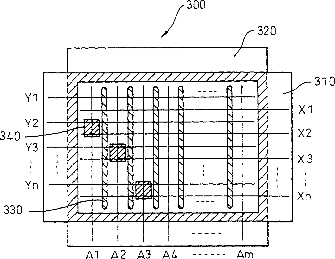
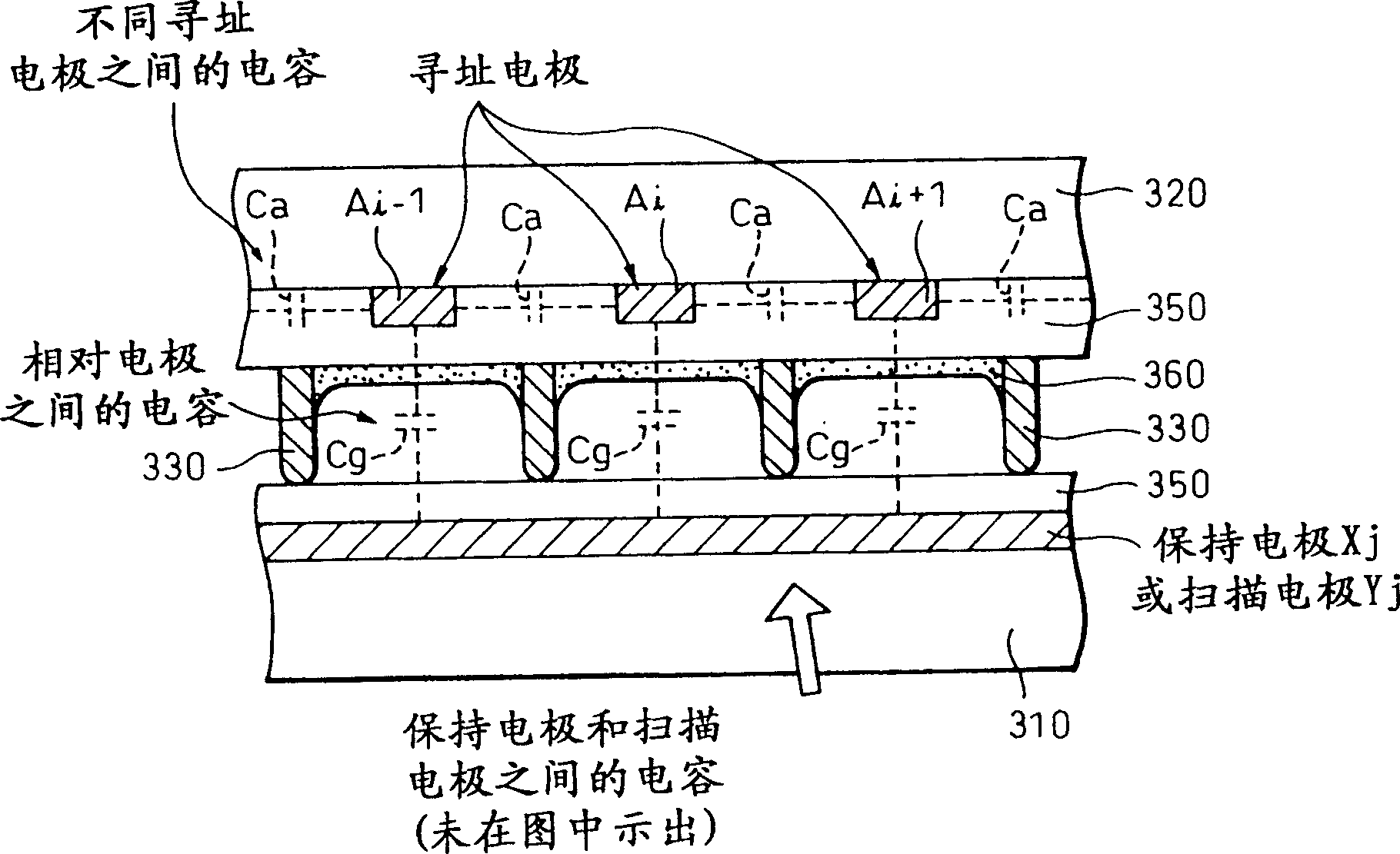
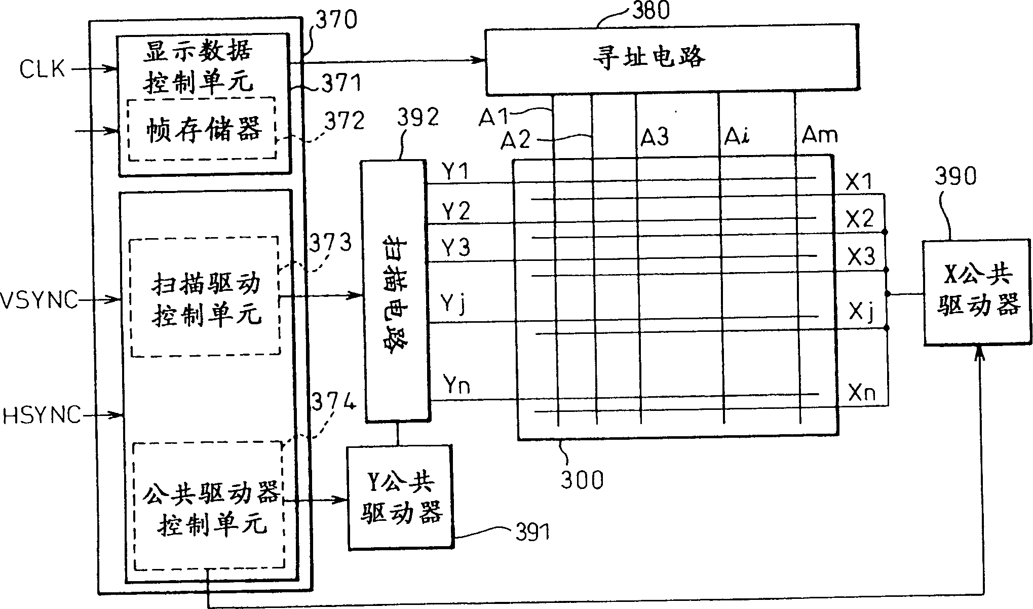
[0093] Refer to the accompanying drawings below ( Figures 11 to 31 ) describes typical preferred embodiments of the present invention. These embodiments are preferably applicable to a drive circuit for driving scan electrodes of a surface discharge AC plasma display panel having three types of electrodes.

[0094] Figure 11 A plan view showing a structure of an assembly mounting a driver IC according to a first embodiment of the present invention. Figure 12 A sectional view showing the structure of an assembly mounting a driver IC according to a first embodiment of the present invention.

[0095] Figure 11 and 12 The first embodiment shown in is an example of applying the driver IC-mounted assembly according to the present invention to the scan electrodes of a surface discharge AC plasma display panel, wherein eight driver IC chips are distributed over two between components that mount the driver IC. However, Figure 11 and 12 A structure of a package 9 mounting a ...


PUM


Abstract

A module, for mounting a driver IC constituting a drive circuit of a display apparatus using a flat display panel, is disclosed, which includes a driver IC chip for driving the display electrodes of the flat display panel and a wiring board electrically connected with the driver IC chip. A module for mounting the driver IC having this configuration comprises a first wiring unit formed with a drive power source system wiring for supplying a power source voltage, which is input to the driver IC chip, for driving the flat display panel through the driver IC chip; a second wiring unit formed with a control system wiring for supplying various signals, which are input to the driver IC chip, for controlling the driver IC chip; and a third wiring unit formed with an output terminal wiring taken out from the driver IC chip and connecting to the display electrodes of the flat display panel.

Description

technical field [0001] The present invention relates to an assembly for mounting a driver IC (Integrated Circuit) constituting a driving circuit to drive display electrodes of a display device using a flat panel display panel, and particularly relates to a new structure for mounting a driver IC assembly capable of providing a signal to the display during operation of the display device. The display panel of the device supplies a stable high current with a predetermined peak value. Background technique [0002] Driver IC mounted components of this structure are generally suitable for display units with large-capacity flat-panel display panels consisting of a large number of display units with capacitive load characteristics, such as plasma display panels (including plasma display panels and peripheral The entire plasma display unit of the circuit is usually called "PDP"), an EL (Electro Luminescence) panel or a large-sized LCD (Liquid Crystal Display) panel. [0003] Recentl...

Claims


Application Information

Patent Timeline
Patent Type & Authority Patents(China)
IPC IPC(8): G02F1/1345G09F9/00G09G3/20G09G3/291G09G3/294G09G3/296H01J11/12H01J11/24H01J11/26H01J11/46H01J11/48H05K1/02
CPCH01L2224/49109H01J2217/49G09G3/299H01L2924/01055G09G3/296H01L2924/3011G09G2310/066H01L2224/48091G09G3/2932H01L2224/48227H01L2224/48237H01L2924/00014H01L2924/00H01J17/34
Inventor 河田外与志青木正心小泉治男
Owner FUJITSU LTD
Learn More