A tooling and a method for cleaning a CMOS image sensor circuit

An image sensor and cleaning device technology, applied in circuits, image communications, color TV components and other directions, can solve the problems of reducing the circuit performance of CMOS image sensors, chip surface damage, etc., and achieves a simple and practical cleaning method, high cleanliness, Actionable effect

Active Publication Date: 2019-01-18
BEIJING MXTRONICS CORP +1
View PDF7 Cites 1 Cited by
  • Summary
  • Abstract
  • Description
  • Claims
  • Application Information

AI Technical Summary

Problems solved by technology

The existing cleaning method is generally manual scrubbing, which can easily cause damage to the chip surface and reduce the performance of the CMOS image sensor circuit

Method used


Image

  • A tooling and a method for cleaning a CMOS image sensor circuit
  • A tooling and a method for cleaning a CMOS image sensor circuit
  • A tooling and a method for cleaning a CMOS image sensor circuit

Examples


Embodiment

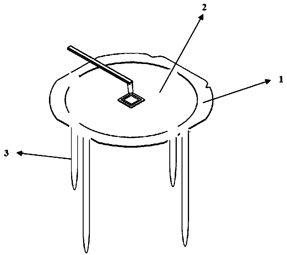
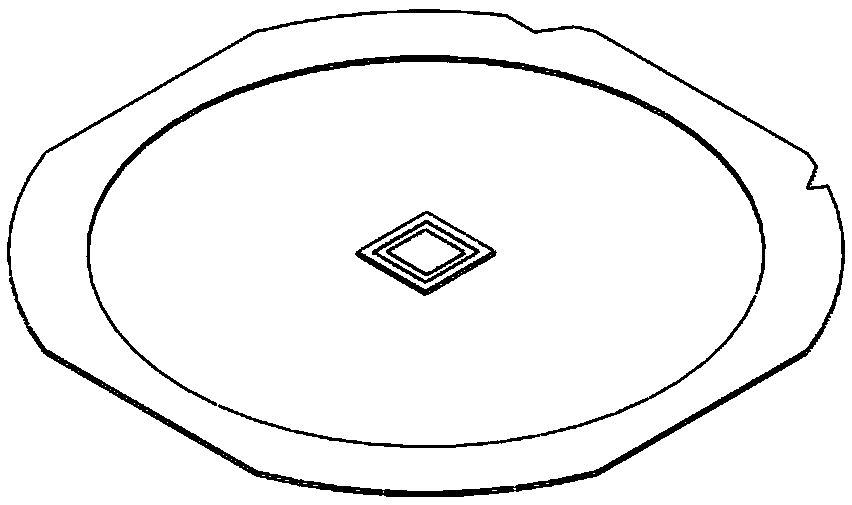
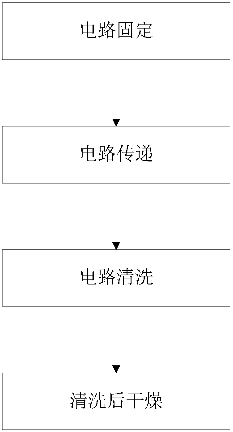
[0040] Tooling is processed according to the present invention. In an environment with a temperature of 23°C and a humidity of 40%, wear an anti-static wristband and brand-new finger cots, pinch the edge of the circuit ceramics with your fingers, and pick up the circuit steadily to prevent your fingers from slipping into the circuit cavity and the circuit from falling. One side of the bottom is the rotation axis, and the circuit is placed on the UV film supported by the dicing material ring in a rotating manner. Fix the circuit without moving, use a scraper to scrape from one end of the circuit to the other end on the lower surface of the UV film, and remove the visible air bubbles on the contact surface between the circuit and the UV film. Remove the fixed dicing material ring, UV film and the overall structure of the CMOS image sensor circuit from the bracket, and place them on the cleaning device workbench. When placed, the moisture on the surface of the CMOS image sensor c...


PUM


Abstract

The invention discloses a tooling and a method for cleaning a CMOS image sensor circuit, and belongs to the CMOS image sensor circuit packaging field. Compared with conventional methods, that invention can quickly and effectively remove dirt, dust and other forms of excess attached on surfaces of a chip, a housing, and a glass cover plate, solves the problem of low reliability of the CMOS image sensor circuit due to the presence of excess in the circuit, which results in the failure of the photosensitive part, and does not affect the bonding strength of the bonding wires inside the circuit. The method of the invention can effectively remove the internal redundancy of the CMOS image sensor circuit, ensure the reliability of the CMOS image sensor circuit after packaging, effectively shortenthe production cycle, and the cleaning method is simple and practical, easy to realize and strong in maneuverability.

Description

technical field [0001] The invention relates to a tooling and a method for cleaning a CMOS image sensor circuit, belonging to the technical field of CMOS image sensor circuit ceramic packaging. Background technique [0002] Compared with traditional CCD imaging technology, CMOS image sensor has the advantages of easy system integration, low power consumption, fast imaging speed, wide response range, strong radiation resistance, and low cost. The prospect of CMOS camera is very broad. [0003] The surface of the chip of the CMOS image sensor circuit is equipped with microlenses, and the surface is uneven. If there are redundant objects, the redundant objects can easily enter the pits and cause one or several pixels to fail. Therefore, the CMOS image sensor circuit is extremely sensitive to excess. Proper cleaning must be carried out before the circuit is capped to remove as much contamination as possible from the chip surface, the inside of the tube, and the glass cover. The...

Claims


Application Information

Patent Timeline
Patent Type & Authority Applications(China)
IPC IPC(8): H01L21/67H01L21/02H04N5/374
CPCH01L21/02082H01L21/67051H04N25/76
Inventor 冯小成李峰李洪剑荆林晓贺晋春井立鹏
Owner BEIJING MXTRONICS CORP
Why Eureka
Try Eureka